Prepare for University Studies & Career Advancement

Condensed Matter Physics

Condensed matter physics explores the diverse and fascinating behaviors of matter in its solid and liquid states, making it one of the most vibrant branches of physics. Grounded in the framework of modern physics, this field investigates how atoms and particles interact collectively to produce phenomena such as superconductivity, magnetism, and crystallinity. It builds upon the quantum foundation established in atomic physics and is deeply intertwined with the concepts of quantum mechanics.

The microscopic structure of solids, including their atomic arrangement and electron configuration, determines a material’s physical properties. These atomic-level descriptions draw upon ideas like quantum superposition and wave-particle duality, which challenge classical conceptions of particle behavior. Phenomena such as quantum tunneling and quantum entanglement play pivotal roles in explaining superconductors, semiconductors, and other complex systems.

To understand the macroscopic behavior of these systems, condensed matter physicists often rely on tools from statistical mechanics. This framework connects microscopic interactions to observable properties like temperature, conductivity, and phase transitions. Many of these insights are enhanced by quantum field theory, which provides a more unified description of how particles and fields interact in large ensembles.

Condensed matter systems often include exotic materials such as those governed by nuclear interactions or composed of complex isotopes studied under radioactivity. Moreover, advanced developments such as high-temperature nuclear fusion and nuclear fission can influence material behaviors at extreme conditions. Interactions at these levels are often governed by fundamental forces and are analyzed in the context of relativity when near-light-speed particles are involved.

Understanding condensed matter also requires insights from particle physics, particularly the behavior of fermions (matter particles) and bosons (force carriers). These particles interact via gauge fields that describe the electromagnetic, weak, and strong forces within materials. The fine balance of these forces gives rise to magnetic ordering, band structure, and other condensed matter phenomena.

At a deeper level, condensed matter is a fertile ground for exploring theoretical principles such as Heisenberg’s uncertainty principle and interpreting the wave function in real-world applications. Whether dealing with semiconductors or superfluids, these principles illuminate the rich complexity of collective particle behavior.

From the atomic lattice to quantum spin systems, condensed matter physics bridges the gap between fundamental theory and practical technology. It informs modern electronics, quantum computing, and materials science, empowering students to explore how underlying principles of the atom shape the macroscopic world. As you journey through this subject, you will connect ideas across atomic structure, subatomic interactions, and quantum principles, forming a robust understanding of the materials that underpin our technological future.

Condensed Matter Physics

Key Concepts in Condensed Matter Physics

1. Crystalline and Amorphous Solids

  • Crystalline Solids: Have a highly ordered, repeating atomic structure (e.g., metals, salts, and semiconductors).
  • Amorphous Solids: Lack long-range order (e.g., glass, plastics).
The arrangement of atoms in a crystal is described by a lattice structure, and imperfections in this structure, known as defects, strongly influence material properties.
A scientific illustration comparing crystalline solids with a highly ordered atomic lattice and amorphous solids with a disordered atomic arrangement.

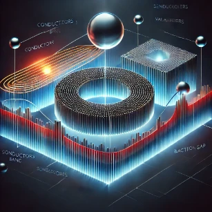
2. Band Theory of Solids

The band theory explains how electrons occupy energy levels in solids:
  • Conductors: Overlapping or partially filled conduction bands allow free electron flow (e.g., metals).
  • Semiconductors: Have a small energy gap between the valence and conduction bands (e.g., silicon).
  • Insulators: Have a large energy gap, preventing electron flow (e.g., diamond).
The band gap influences electrical, thermal, and optical properties.
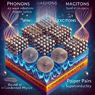
Band Theory of Solids, showing the distinct energy band structures of conductors, semiconductors, and insulators.

3. Quasiparticles

In complex systems, collective excitations behave like particles called quasiparticles. They simplify the description of interactions in solids.
  • Phonons: Quanta of lattice vibrations (heat carriers).
  • Magnons: Quanta of spin waves in magnetic materials.
  • Excitons: Bound states of electrons and holes in semiconductors.
  • Cooper Pairs: Paired electrons in superconductors.
Quasiparticles in condensed matter physics, including phonons, magnons, excitons, and Cooper pairs

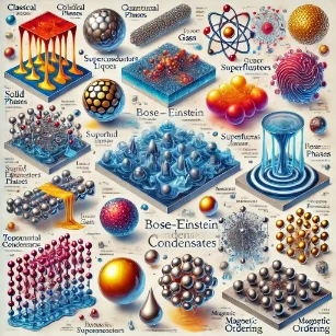
4. Phases of Matter and Phase Transitions

CMP studies different states of matter and their transitions:
  • Classical Phases: Solid, liquid, gas.
  • Quantum Phases: Superconductors, superfluids, Bose-Einstein condensates (BECs).
  • Topological Phases: Exotic states characterized by global properties, not local symmetries.
Phase transitions occur when a material changes from one state to another, such as melting or magnetic ordering, often characterized by symmetry breaking.
Different phases of matter and their transitions.

5. Superconductivity

Superconductivity is a phenomenon where certain materials exhibit zero electrical resistance and expel magnetic fields (Meissner effect) below a critical temperature.
  • Conventional Superconductors: Explained by BCS theory, where electrons form Cooper pairs.
  • High-Temperature Superconductors (HTS): Materials that superconduct at higher temperatures, whose mechanisms are still not fully understood.
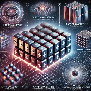
Superconductivity, featuring a levitating superconductor above a magnet due to the Meissner effect.

6. Magnetism

CMP studies various forms of magnetism in materials:
  • Ferromagnetism: Magnetic moments align in the same direction (e.g., iron).
  • Antiferromagnetism: Adjacent moments align oppositely, canceling out.
  • Paramagnetism: Materials become magnetic only in external fields.
  • Spintronics: Exploits electron spin for data storage and electronics.
Different Types of Magnetism, including ferromagnetism, antiferromagnetism, paramagnetism, and spintronics.

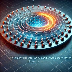
7. Topological Insulators

Topological insulators are materials that behave as insulators in their interior but conduct electricity on their surfaces or edges due to topological properties. These materials have promising applications in quantum computing and spintronics.
Topological Insulator. It visually represents its insulating interior and conductive surface states, highlighting its applications in quantum computing and spintronics.

Experimental Techniques in Condensed Matter Physics

1. X-ray Crystallography

Used to determine the atomic structure of crystalline materials by analyzing the diffraction patterns of X-rays passing through the sample.

2. Scanning Tunneling Microscopy (STM)

A technique that allows imaging and manipulating atoms on a surface by measuring quantum tunneling currents.

3. Angle-Resolved Photoemission Spectroscopy (ARPES)

Used to study the electronic structure of materials by measuring the energy and momentum of electrons ejected by light.

4. Neutron and X-ray Scattering

Used to study the arrangement of atoms and magnetic properties.

5. Transport Measurements

Involves measuring electrical, thermal, and magnetic properties to study superconductivity, magnetism, and conductivity.

Applications of Condensed Matter Physics

  1. Semiconductor Devices: Foundation for modern electronics (transistors, diodes, integrated circuits).
  2. Superconductors: Used in MRI machines, maglev trains, and quantum computers.
  3. Magnetic Materials: Essential for data storage (hard drives), electric motors, and transformers.
  4. Photonic Materials: Enable lasers, LEDs, and solar cells.
  5. Nanotechnology: Development of nanoscale devices and materials.

Five Numerical Examples

Example 1: Estimating the Fermi Energy of Copper

Problem: Calculate the Fermi energy of copper. Given the electron density n=8.5×1028electrons/m3n = 8.5 \times 10^{28} \, \text{electrons/m}^3.Solution: EF=22m(3π2n)2/3E_F = \frac{\hbar^2}{2m} (3\pi^2 n)^{2/3} EF=(1.055×1034)22×9.11×1031(3π2×8.5×1028)2/3E_F = \frac{(1.055 \times 10^{-34})^2}{2 \times 9.11 \times 10^{-31}} (3\pi^2 \times 8.5 \times 10^{28})^{2/3} EF7.0eVE_F \approx 7.0 \, \text{eV}

Answer:

The Fermi energy of copper is approximately 7.0 eV.

Example 2: Band Gap Energy in Semiconductors

Problem: A photon with energy 2.5eV is absorbed by a semiconductor. Will it excite an electron across a 1.1 eV band gap? Solution: Since 2.5 eV>1.1eV, the photon has enough energy to excite an electron, the photon has enough energy to excite an electron.Answer: Yes, the photon can excite an electron across the band gap.

Example 3: Critical Temperature for Superconductivity

Problem: Calculate the critical temperature (Tc) for a superconductor with an energy gap Δ=2meVSolution: Δ=1.76kBTc\Delta = 1.76 k_B T_c Tc=Δ1.76kB=2×10³eV1.76×8.617×105eV/K13.2KT_c = \frac{\Delta}{1.76 k_B} = \frac{2 \times 10^{-3} \, \text{eV}}{1.76 \times 8.617 \times 10^{-5} \, \text{eV/K}} \approx 13.2 \, \text{K}Answer: The critical temperature is approximately 13.2 K.

Example 4: Magnetic Moment in a Ferromagnet

Problem: If each iron atom has a magnetic moment of 2.2 μB and the number density is 8.5×1028atoms/m38.5 \times 10^{28} \, \text{atoms/m}^3, find the magnetization. Solution: M=nμM = n \mu M=8.5×1028×2.2×9.27×10241.73×106A/mM = 8.5 \times 10^{28} \times 2.2 \times 9.27 \times 10^{-24} \approx 1.73 \times 10^{6} \, \text{A/m}Answer The magnetization is 1.73×10⁶A/m

Example 5: Phonon Energy

Problem: Find the energy of a phonon with frequency 5×10¹²Hz Solution: E=hν=6.626×1034×5×1012=3.31×10²¹JE = h \nu = 6.626 \times 10^{-34} \times 5 \times 10^{12} = 3.31 \times 10^{-21} \, \text{J}Answer: The phonon energy is 3.31×10²¹J

Why Study Condensed Matter Physics

Understanding Solids and Liquids at the Microscopic Level

Condensed matter physics explores the physical properties of matter in solid and liquid phases. Students investigate how atoms and electrons interact in ordered and disordered systems. This field explains the behavior of materials ranging from metals to superconductors. It offers insights into both fundamental science and technological applications.

Crystalline Structures and Band Theory

Students study how atoms are arranged in crystals and how this affects electrical, optical, and mechanical properties. Band theory explains how electrons move through solids and distinguishes conductors, insulators, and semiconductors. This knowledge is vital for electronics, optoelectronics, and nanotechnology. It enables precise control over material behavior.

Emergent Phenomena and Material Properties

Condensed matter physics reveals collective effects like superconductivity, magnetism, and phase transitions. Students explore how simple interactions at the atomic scale lead to complex macroscopic behaviors. This understanding supports the development of new functional materials. It illustrates the richness and complexity of matter.

Experimental Techniques and Characterization

Students gain experience with tools like X-ray diffraction, scanning tunneling microscopy, and electron spectroscopy. These methods allow for detailed study of structure and electronic properties. Hands-on skills prepare students for careers in research, materials science, and engineering. They enable accurate investigation of microscopic phenomena.

Pathway to Future Technologies

Condensed matter physics underlies innovations in quantum materials, flexible electronics, and energy storage. Students who master this subject are prepared to work on next-generation technologies. It bridges theoretical physics with engineering and applied science. It empowers students to shape the future of materials and devices.


Conclusion

Condensed Matter Physics is a cornerstone of modern physics and technology. It explains how microscopic interactions among atoms and electrons give rise to the diverse physical properties of materials. By understanding these phenomena, CMP has led to revolutionary technologies, including semiconductors, superconductors, and magnetic materials. Ongoing research in quantum materials, nanotechnology, and topological phases continues to drive innovation and discovery in this dynamic field.

Review Questions and Answers:

1. What is condensed matter physics and why is it important?
Answer: Condensed matter physics is the study of the physical properties of solids and liquids, focusing on how atoms and electrons interact in large ensembles. It is crucial for understanding phenomena like conductivity, magnetism, and superconductivity, which underpin modern technology.

2. How do crystal structures influence the properties of materials?
Answer: Crystal structures determine the arrangement of atoms in a solid, influencing properties such as density, electrical conductivity, and mechanical strength. The symmetry and periodicity of the lattice directly affect the material’s electronic band structure and optical behavior.

3. What role does band theory play in condensed matter physics?
Answer: Band theory explains the behavior of electrons in solids by describing allowed and forbidden energy regions (bands and gaps). It is fundamental for understanding electrical conductivity in metals, semiconductors, and insulators, and for designing electronic devices.

4. How is superconductivity explained within the framework of condensed matter physics?
Answer: Superconductivity arises when electrons form Cooper pairs at low temperatures, resulting in zero electrical resistance and the expulsion of magnetic fields. This quantum phenomenon is explained by theories such as the BCS theory, which describes the attractive interaction between electrons mediated by lattice vibrations.

5. What is the significance of quasiparticles in condensed matter systems?
Answer: Quasiparticles are effective entities that represent collective excitations in a material, such as phonons or magnons. They simplify the complex interactions in solids, enabling physicists to model and predict thermal, electrical, and magnetic properties more accurately.

6. How does magnetism emerge from electron interactions in solids?
Answer: Magnetism in solids originates from the spin and orbital motion of electrons. The alignment or anti-alignment of electron spins due to exchange interactions leads to various magnetic behaviors, including ferromagnetism, antiferromagnetism, and paramagnetism.

7. What experimental techniques are commonly used to study condensed matter systems?
Answer: Techniques such as X-ray diffraction, neutron scattering, electron microscopy, and spectroscopy (including ARPES and Raman spectroscopy) are used to probe crystal structures, electron dynamics, and vibrational modes, providing insights into material properties at the atomic scale.

8. How do defects and impurities affect the properties of condensed matter?
Answer: Defects and impurities can significantly alter a material’s physical properties by disrupting the periodic lattice, affecting electron mobility and scattering. They can introduce localized energy states, modify conductivity, and even enhance certain properties like catalytic activity.

9. In what ways do nanomaterials differ from their bulk counterparts in condensed matter physics?
Answer: Nanomaterials exhibit unique properties due to quantum confinement and a high surface-to-volume ratio. These differences lead to altered electronic, optical, and magnetic behaviors compared to bulk materials, opening up applications in medicine, electronics, and energy storage.

10. How does temperature influence phase transitions in condensed matter systems?
Answer: Temperature affects the energy and motion of atoms, leading to phase transitions such as melting, crystallization, or superconducting transitions. As temperature changes, the balance between thermal energy and interatomic forces shifts, resulting in different structural and electronic phases.

Thought-Provoking Questions and Answers

1. How might advances in condensed matter physics revolutionize the development of quantum computers?
Answer: Advances in condensed matter physics could lead to the discovery of new materials that exhibit robust quantum coherence and low decoherence rates, crucial for quantum computing. Materials such as topological insulators and superconductors can host exotic quasiparticles that enable fault-tolerant qubits, potentially revolutionizing computational power and speed.

2. In what ways could engineered defects in materials be harnessed to improve device performance?
Answer: Engineered defects can be used to tailor material properties deliberately, such as by introducing energy levels that enhance conductivity or luminescence. For example, defect engineering in semiconductors can improve the efficiency of LEDs and solar cells, while controlled impurity doping can optimize the performance of transistors and sensors.

3. How do emergent phenomena in complex materials challenge our current theoretical models in condensed matter physics?
Answer: Emergent phenomena, such as high-temperature superconductivity and quantum spin liquids, arise from collective interactions that cannot be easily predicted by simple models. These challenges push theorists to develop more sophisticated frameworks that account for many-body interactions, nonlinearity, and quantum entanglement in complex systems.

4. What potential breakthroughs could occur by merging condensed matter physics with nanotechnology?
Answer: Merging condensed matter physics with nanotechnology could lead to the creation of ultra-efficient energy materials, novel drug delivery systems, and miniaturized electronic devices. At the nanoscale, materials exhibit quantum effects that allow for unprecedented control over electronic, optical, and thermal properties, opening up new avenues for innovation.

5. How might the study of topological phases in condensed matter lead to new types of electronic devices?
Answer: Topological phases offer robust edge states that are resistant to defects and disorder. This property can be exploited to develop electronic devices with minimal energy loss and enhanced stability. Topological insulators and superconductors could pave the way for dissipationless electronics and quantum computing components that are less susceptible to environmental noise.

6. In what ways can the study of soft condensed matter, such as polymers and colloids, impact everyday technology?
Answer: Soft condensed matter research has direct implications for everyday technology, influencing the development of flexible electronics, advanced coatings, and biomedical devices. Understanding the dynamics and self-assembly of polymers and colloids can lead to innovations in material design, impacting industries ranging from consumer electronics to healthcare.

7. How does quantum confinement in low-dimensional systems alter the physical properties of materials?
Answer: Quantum confinement in low-dimensional systems, such as quantum dots or nanowires, restricts electron movement and leads to discrete energy levels. This results in altered optical absorption, emission spectra, and electrical conductivity compared to bulk materials, enabling applications in lasers, displays, and photovoltaic devices.

8. What are the implications of discovering new phases of matter, like time crystals, for condensed matter physics?
Answer: Discovering new phases of matter such as time crystals challenges conventional notions of equilibrium and symmetry. These findings could lead to a deeper understanding of nonequilibrium dynamics and open up possibilities for developing materials with novel time-dependent properties, potentially impacting energy storage and signal processing technologies.

9. How can advances in computational modeling enhance our understanding of strongly correlated electron systems?
Answer: Advances in computational modeling enable the simulation of strongly correlated electron systems with high accuracy. Techniques like quantum Monte Carlo methods and density functional theory help unravel the complex interactions in these systems, leading to predictions of new materials with exotic properties and guiding experimental discoveries in superconductivity and magnetism.

10. What role might artificial intelligence play in accelerating research in condensed matter physics?
Answer: Artificial intelligence can analyze vast datasets from experiments and simulations to identify patterns and predict material behaviors that may be missed by traditional methods. Machine learning algorithms can optimize material properties, suggest new compounds, and accelerate the discovery of novel phases, thereby transforming research methodologies in condensed matter physics.

11. How could the manipulation of electron–phonon interactions lead to the development of materials with tailored thermal properties?
Answer: By controlling electron–phonon interactions, researchers can design materials with specific thermal conductivities. This could lead to improved thermoelectric materials for energy conversion or better thermal insulators for electronic devices, enabling more efficient heat management in a variety of applications.

12. What challenges must be overcome to fully harness the potential of 2D materials like graphene in practical applications?
Answer: To fully harness 2D materials like graphene, challenges such as scalable production, integration with existing technologies, and controlling defects and grain boundaries must be addressed. Overcoming these obstacles requires advances in synthesis techniques, material processing, and a deeper understanding of the interaction between 2D materials and their environment.

Numerical Problems and Solutions

1. A crystal lattice has a cubic unit cell with an edge length of 0.5 nm. Calculate the volume of the unit cell.
Solution:
Solution:
Volume = a³ = (0.5 × 10⁻⁹ m)³ = 0.125 × 10⁻²⁷ m³ = 1.25 × 10⁻²⁸ m³.

2. Given a semiconductor with a band gap of 1.1 eV, calculate the wavelength of light corresponding to this band gap. (Use E = hc/λ, h = 4.1357×10⁻¹⁵ eV·s, c = 3×10⁸ m/s)
Solution:
Solution:
λ = hc/E = (4.1357×10⁻¹⁵ eV·s × 3×10⁸ m/s) / 1.1 eV ≈ (1.2407×10⁻⁶ eV·m) / 1.1 eV ≈ 1.128×10⁻⁶ m or 1128 nm.

3. A superconducting material has a critical temperature of 9 K. If the energy gap at 0 K is approximately 1.76kBTc, calculate the energy gap in meV. (kB = 8.617×10⁻⁵ eV/K)
Solution:
Solution:
Energy gap = 1.76 × kB × Tc = 1.76 × 8.617×10⁻⁵ eV/K × 9 K ≈ 1.36×10⁻³ eV ≈ 1.36 meV.

4. Calculate the density of a material with a molar mass of 63.5 g/mol and a face-centered cubic (FCC) structure, given that the lattice parameter is 0.361 nm and there are 4 atoms per unit cell. (Avogadro’s number = 6.022×10²³ mol⁻¹)
Solution:
Solution:
Volume of unit cell = (0.361×10⁻⁹ m)³ ≈ 4.71×10⁻²⁹ m³.
Mass per unit cell = (4 atoms × 63.5×10⁻³ kg/mol) / (6.022×10²³) ≈ (254×10⁻³) / (6.022×10²³) ≈ 4.22×10⁻²⁶ kg.
Density = mass/volume ≈ 4.22×10⁻²⁶ kg / 4.71×10⁻²⁹ m³ ≈ 896 kg/m³.

5. For a material with a Debye temperature of 300 K, estimate the Debye frequency using ω_D = kBΘ_D/ħ. (ħ = 1.055×10⁻³⁴ J·s, kB = 1.38×10⁻²³ J/K)
Solution:
Solution:
ω_D = (1.38×10⁻²³ J/K × 300 K) / (1.055×10⁻³⁴ J·s) ≈ (4.14×10⁻²¹ J) / (1.055×10⁻³⁴ J·s) ≈ 3.92×10¹³ s⁻¹.

6. A thin film of a magnetic material has a thickness of 50 nm and a magnetic moment per unit volume of 8×10⁵ A/m. Calculate the total magnetic moment per square meter of film surface.
Solution:
Solution:
Magnetic moment per area = moment per volume × thickness = 8×10⁵ A/m × 50×10⁻⁹ m = 4×10⁻² A·m per m².

7. Determine the effective mass of electrons in a semiconductor if the conduction band curvature gives m = 0.1 mₑ, where mₑ = 9.11×10⁻³¹ kg.*
Solution:
Solution:
m* = 0.1 × 9.11×10⁻³¹ kg = 9.11×10⁻³² kg.

8. A nanomaterial has a thermal conductivity of 150 W/m·K. If a temperature difference of 10 K is applied across a 100 nm thick sample, calculate the heat flux (W/m²) through the material.
Solution:
Solution:
Heat flux = (Thermal conductivity × Temperature difference) / thickness
= (150 W/m·K × 10 K) / (100×10⁻⁹ m) = (1500 W/m) / (100×10⁻⁹ m) = 1.5×10¹³ W/m².

9. In a metal, the electron concentration is 8.5×10²⁸ m⁻³. Calculate the Fermi energy using E_F = (ħ²/2mₑ)(3π²n)^(2/3). (ħ = 1.055×10⁻³⁴ J·s, mₑ = 9.11×10⁻³¹ kg)
Solution:
Solution:
First, calculate (3π²n)^(2/3):
3π²n = 3π²×8.5×10²⁸ ≈ 3×9.87×8.5×10²⁸ ≈ 251.7×10²⁸,
(251.7×10²⁸)^(2/3) ≈ (2.517×10³⁰)^(2/3) ≈ 6.3×10²⁰.
Then, E_F = (1.055²×10⁻⁶⁸ J²·s²)/(2×9.11×10⁻³¹ kg) × 6.3×10²⁰
≈ (1.113×10⁻⁶⁸)/(1.822×10⁻³⁰) × 6.3×10²⁰ ≈ 6.1×10⁻¹⁹ J
Convert to eV: 6.1×10⁻¹⁹ J / 1.602×10⁻¹⁹ ≈ 3.8 eV.

10. A phonon in a crystal has a wavelength of 2 nm. If the speed of sound in the material is 5000 m/s, calculate the phonon energy. (Use E = hv/λ with h = 6.626×10⁻³⁴ J·s)
Solution:
Solution:
Frequency v = speed / wavelength = 5000 m/s / (2×10⁻⁹ m) = 2.5×10¹² Hz.
Then, E = h×v = 6.626×10⁻³⁴ J·s × 2.5×10¹² Hz = 1.6565×10⁻²¹ J.

11. For a 2D electron gas in a semiconductor, the density of states per unit area is given by D(E) = m/(πħ²). Calculate D(E) for m = 0.07 mₑ. (Use mₑ = 9.11×10⁻³¹ kg and ħ = 1.055×10⁻³⁴ J·s)
Solution:
Solution:
m = 0.07 × 9.11×10⁻³¹ kg = 6.377×10⁻³² kg.
D(E) = m*/(πħ²) = 6.377×10⁻³² kg / (π × (1.055×10⁻³⁴ J·s)²)
= 6.377×10⁻³² / (π × 1.113×10⁻⁶⁸) ≈ 1.83×10³⁶ J⁻¹·m⁻².

12. A sample of a novel material has an electrical conductivity of 1×10⁴ S/m. If a voltage of 5 V is applied across a 1 cm thick sample with an area of 1×10⁻⁴ m², calculate the current flowing through the material.
Solution:
Solution:
First, calculate the resistance R = (thickness)/(σ × area) = (0.01 m)/(1×10⁴ S/m × 1×10⁻⁴ m²) = 0.01/1 = 0.01 Ω.
Then, using Ohm’s law, I = V/R = 5 V / 0.01 Ω = 500 A.