
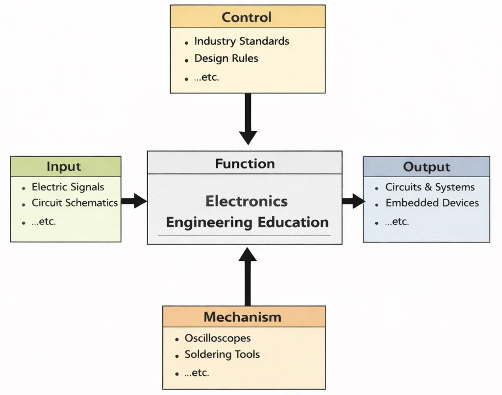
Electronics Engineering Education, at its core, teaches students to turn invisible behavior into visible, testable design. The diagram’s left-to-right flow captures the discipline’s rhythm: start with signals and schematic ideas, interpret them through the “grammar” of standards and design constraints, and then use instruments and fabrication tools to verify what the math predicts. The central Function box represents this training as a disciplined conversion of curiosity into competence—where learners repeatedly model, measure, troubleshoot, and refine until circuits stop being drawings and become dependable systems. Over time, the outputs are not only devices, but also a mindset: careful reasoning, evidence-based debugging, and the habit of building things that work in the real world.
Electronics Engineering is the backbone of modern digital civilization, providing the tools and systems that power computing devices, telecommunications, automation, and intelligent systems. It forms a major pillar of Electrical and Electronic Engineering, enabling the design and development of everything from smartphones and sensors to satellites and industrial controllers. As such, it integrates knowledge of semiconductors, circuit design, signal transmission, and embedded systems.
The journey begins with understanding how signals behave, making Signal Processing a vital area of study. Signal conditioning and transformation are central to applications in Communication Engineering, which deals with data transmission across channels from local devices to global networks. Reliable monitoring and calibration systems in Instrumentation and Measurement help ensure signal fidelity and safe operation of electronics in sensitive environments.
The intelligence of devices owes much to Control Systems Engineering and innovations in Embedded Systems and Microelectronics, where circuit miniaturization supports smart applications in wearables, medical implants, and autonomous systems. These advances connect directly with broader cyber-physical systems explored under the Internet of Things (IoT) and Smart Technologies.
Emerging technologies such as Quantum Electronics are pushing the boundaries of traditional electronics, enabling new forms of computation and secure communication. Meanwhile, Robotics and Automation in E&E depend on precision electronics for sensory feedback, actuation, and real-time control.
Practical applications extend to energy infrastructure, where electronics underpin Power Systems Engineering and help regulate Renewable Energy and Energy Storage systems. Students interested in sustainability will also find synergy with Environmental Engineering, particularly in the monitoring of ecosystems through advanced sensing and data acquisition.
Examples include electronic devices used in Air Quality Engineering and Water Resources Engineering, where real-time data is critical to public health and resource management. Sophisticated analysis and remote control are supported through Environmental Monitoring and Data Analysis.
The interface between electronics and biomedical science is another fast-growing area. Innovations in Biomedical Electronics have revolutionized patient monitoring, diagnostics, and therapeutic interventions. From cardiac pacemakers to neural prosthetics, electronics continue to enhance quality of life and extend medical capabilities.
On a broader scale, electronics engineers contribute to sustainable infrastructure by supporting Green Building and Sustainable Design and managing electronic systems within Industrial Ecology and Circular Economy frameworks. Related developments are found in Renewable Energy Systems Engineering and optimized waste processes in Waste Management Engineering.
As electronics permeate every facet of industry and society, the role of engineers becomes increasingly interdisciplinary. By linking design, innovation, and responsible application, students of Electronics Engineering are empowered to build transformative technologies for a connected, efficient, and sustainable future.
Interactive Circuit Simulator: RC Filter Bode Magnitude Response
Adjust Resistance (\(R\)), Capacitance (\(C\)), and topology mode to evaluate the half-power cutoff frequency (\(f_c\)), decibel attenuation roll-off (\(-20\,\text{dB/decade}\)), and logarithmic frequency response spectrum.

The image portrays a high-tech electronics lab where a suited engineer examines a luminous integrated circuit at the center of a vast circuit-board “workbench.” Around the chip, component packages and traces suggest real hardware design, while holographic overlays show network diagrams, waveforms, and technical panels—hinting at simulation, testing, and system integration. Robotic arms and instrument-like devices reinforce the idea of precision fabrication and automated inspection. Overall, it visually links core electronics (chips, circuits, components) with today’s connected world of AI, IoT, and embedded systems.
Electronics Engineering: Curriculum Roadmap & Cluster Navigation
Electrical & Electronic Engineering – Overview
Establishes the foundational parent discipline, framing macro-scale power distribution alongside low-voltage signal dynamics across physical systems.
Electronics Engineering (Current Page)
Focuses on semiconductor physics, analog/digital circuit architectures, and chip layout to manipulate low-voltage electronic signals.
Embedded Systems & Microelectronics
Explores how circuit designs are miniaturized into silicon microcontrollers and System-on-Chip (SoC) platforms to run dedicated firmware.
Signal Processing
Applies mathematical algorithms and filtering techniques to convert raw analog sensor voltages into clean, digital data streams.
Communication Engineering
Extends circuit theory into RF transmission, modulation schemes, and network protocols for long-distance wired and wireless data transfer.
Control Systems Engineering
Utilizes electronic feedback networks and operational amplifiers to regulate dynamic hardware, ensuring precise mechanical behavior.
Instrumentation & Measurement
Focuses on sensor interface design, ADC calibration, and instrument front-ends to capture high-fidelity physical data.
IoT & Smart Technologies
Connects low-power embedded electronic nodes to cloud infrastructures via ultra-low-power wireless networking modules.
Power Systems Engineering
Applies high-power semiconductor electronics (IGBTs, Thyristors) to control grid voltage, transformation, and distribution safety.
Renewable Energy & Energy Storage
Engineers solid-state power conversion circuits and battery management ICs to integrate solar and wind into energy grids.
Robotics & Automation in EE
Merges sensory electronics, motor drive circuits, and real-time processing to actuate autonomous physical mechanisms.
Quantum Electronics
Pushes electronic boundaries by controlling electron spin and quantum tunneling to build ultra-fast next-generation devices.
Biomedical Electronics
Designs bio-compatible, ultra-low-noise electronic interfaces for biological signal acquisition and life-saving implantable devices.
Key Areas in Electronics Engineering
Electronics engineering is a vast and rapidly evolving discipline that extends far beyond simple circuit design. It encompasses the study and application of electronic systems across multiple domains, each with its own unique challenges, technologies, and innovation landscapes. The core areas outlined below reflect both fundamental and cutting-edge sectors where electronics engineers make an impact.
Electronic Circuits
- Analog Circuits: These circuits process continuous signals and are fundamental in designing amplifiers for audio equipment, oscillators in radios, voltage regulators, and precision sensors. Modern analog circuit design emphasizes low-noise performance, high dynamic range, and energy efficiency to support applications like biomedical instrumentation, environmental monitoring, and sensor arrays.
- Digital Circuits: Operating with discrete voltage levels, digital circuits form the backbone of microprocessors, memory modules, digital signal processors (DSPs), and logic gates. Engineers design these circuits using hardware description languages (HDLs), focusing on clock domains, timing closure, low-power modes, and secure boot mechanisms in embedded systems.
- Mixed-Signal Circuits: These hybrid circuits combine analog and digital domains to handle real-world data in systems like audio codecs, analog-to-digital converters (ADCs), digital-to-analog converters (DACs), and RF transceivers. Design considerations include clock jitter, isolation, crosstalk reduction, and programmable calibration strategies.
Consumer Electronics
- Smartphones and Tablets: Engineers integrate multiple subsystems—touchscreen control, multi-lens camera interfaces, RF front ends for 4G/5G/Wi-Fi, battery management systems, and secure storage/crypto modules into compact, power-efficient packages.
- Televisions and Home Entertainment Systems: Advances in display technologies—OLED, QLED, and 8K Ultra HD—as well as embedded smart functionality (streaming, voice assistants, edge AI) are driven by high-performance video processors, backlight inverters, and digital audio systems.
- Wearable Devices: Electronics engineers miniaturize PCBs, design low-power radio modules (BLE, NFC), integrate biometric sensors, and manage power budgets in devices like fitness trackers, smartwatches, and AR glasses that demand reliability over extended wear.
Medical Electronics
- Diagnostic Devices: Innovations in MRI scanners, CT machines, and X-ray systems rely on precision timing, high-voltage electronics, RF coil tuning, digital signal reconstruction, and electromagnetic shielding strategies.
- Therapeutic Devices: Pacemakers and defibrillators use high-reliability circuits, telemetry for remote monitoring, low-risk power architectures, and implantable-grade packaging. Insulin pumps require safe, programmable control loops and fault tolerance.
- Wearable Health Monitors: Devices for tracking heart rate, blood oxygen, glucose levels, and more rely on custom analog front ends, photoplethysmography (PPG) sensors, secure wireless transmission, and robust algorithmic interpretation.
Industrial Applications
- Sensors and Actuators: Engineers deploy pressure transducers, strain gauges, and temperature sensors, alongside actuators like stepper and servo motors. Signal conditioning, noise rejection, and rugged enclosure design are key.
- Programmable Logic Controllers (PLCs): These systems support factory automation using ladder logic or structured text, offering modular I/O, industrial fieldbus support, and real-time control loops under IEC 61131 standards.
- Robotics: Control engineers develop motor drivers, sensor feedback loops, field-oriented control (FOC) for motors, and integrated electronics for robotic manipulators and autonomous platforms.
Embedded Systems
- Applications such as automotive ABS systems require real-time responsiveness, fail-safe routines, and deterministic timing.
- IoT devices rely on modular radio interfaces (Zigbee, LoRaWAN, Wi-Fi), secure firmware rollout with OTA updates, and hardware-backed encryption.
- Real-time embedded platforms support avionics communication buses (ARINC 429, CAN FD), RTOS scheduling, and certification for safety-critical deployments.
Power Electronics
- Converters and Inverters are essential in solar panel installations, EV charge ports, and uninterruptible power supplies (UPS). Design focuses on high-efficiency switching (GaN, SiC), thermal management, and EMI control.
- Motor Drives enable variable frequency drives (VFDs), sensorless control, regenerative braking, and field-oriented control for industrial and vehicle motors.
- Power Supplies for electronics involve AC/DC and DC/DC converters with isolation, feedback loops, ripple suppression, and overload protection.
Communication Electronics
- Wireless Communication integrates RF design, phased-array antenna systems, filters, and modulated transceivers for cellular, Wi-Fi, and short-range protocols.
- Satellite Systems involve high-linearity RF front ends, signal tracking, Doppler compensation, and robust modulators for GPS and broadcast uplinks.
- Optical Communication uses high-speed laser drivers, photodetectors, transimpedance amplifiers, and optical multiplexers in fiber-optic links.
Microelectronics
- Integrated Circuits (ICs): Deep-submicron CMOS, embedded memory (SRAM, eFlash), analog blocks, PLLs, and ESD protections form the cores of modern electronics.
- Microprocessors and Microcontrollers: From ARM cores to RISC-V designs, embedded systems integrate real-time peripherals, DMA, and hardware accelerators.
- Nanoelectronics: Cutting-edge research continues into tunnel FETs, molecule-scale devices, and carbon-based electronics to push power and performance boundaries.
Tools and Techniques in Electronics Engineering
Electronics engineering is propelled forward by an array of sophisticated tools, methodologies, and workflows that enable design, testing, and deployment of cutting-edge systems. From simulation and prototyping to fabrication and measurement, these tools empower engineers to iterate quickly, ensure reliability, and meet evolving performance and regulatory demands. Below is a comprehensive exploration of the key tools and techniques shaping modern electronics engineering.
Simulation and Design Software
- SPICE (Simulation Program with Integrated Circuit Emphasis): This analog circuit simulator remains indispensable for evaluating performance metrics such as voltage gain, noise, distortion, and frequency response in amplifier designs, filters, RF circuits, and sensor interfaces. Engineers use variants like LTspice, PSpice, and Ngspice to test large-signal, transient, and AC analysis before physical prototyping.
- MATLAB and Simulink: Beyond simple signal processing, these tools support model-based design across domains—from control systems and DSP to communications and power electronics. Engineers build block-diagram simulations, co-simulate with hardware-in-the-loop (HIL) setups, and automatically generate code for microcontrollers, FPGAs, and embedded processors.
- PCB Design Software: Layout tools such as KiCad, Eagle, and Altium Designer enable the creation of intricate multi-layer boards, handling component placement, signal integrity, thermal planning, and manufacturable outputs. Advanced features include auto-router, DFM (Design for Manufacturing) checks, and 3D board visualization to ensure form factor compatibility and EMI compliance.
Prototyping Tools
- Breadboards and Perfboards: Ideal for rapid circuit assembly and debugging during early development stages. Engineers can test component behavior, adjust schematics, and validate circuit topology without soldering. Perfboards then transition working prototypes to more permanent, customizable designs using discrete soldered components.
- 3D Printing: Not just for aesthetics—additive manufacturing creates custom enclosures, mounting fixtures, cable strain reliefs, and even functional components like heat sinks or RF chokes. Rapid iteration supports quick validation of fit, form, and mechanical integration before going to mold or sheet metal fabrication.
Testing and Measurement Instruments
- Oscilloscopes: From analog to high-bandwidth digital models, oscilloscopes visualize waveform characteristics like amplitude, timing, noise, and signal integrity. Features such as deep memory, serial bus decoding, and protocol analysis (e.g., I2C, SPI, CAN) are pivotal for digital and mixed-signal debugging.
- Multimeters: A must-have tool for measuring DC and AC voltage, current, and resistance. Advanced models include features such as frequency measurement, capacitance testing, diode and transistor test modes, and True RMS measurement for accurate readings under complex loads.
- Logic Analyzers: These instruments capture and decode parallel and serial digital signals in complex IC systems—extracting data from buses, SPI, I2C, and UART interfaces. Engineers use them to debug communication protocols, timing issues, and logic-level handshakes.
Fabrication Techniques
- Semiconductor Fabrication: Involves precision processes like photolithography, doping, etching, and metallization to create integrated circuits at nanometer scales. Engineers design masks, simulate process variation, and validate yield for IC fabrication in foundries using design rule checks (DRC) and layout versus schematic (LVS) tools.
- Soldering: Mastery of soldering techniques—hand soldering, reflow soldering, wave soldering, and surface mount technology (SMT)—is essential for assembling PCBs. Engineers optimize solder paste profiles, component placement tolerances, and inspection methods (e.g., X-ray, AOI) to ensure thermal reliability and mechanical robustness.
Contemporary Computational Paradigms in Modern Electronics
Modern microelectronics and high-speed electronic systems face physical limits where classical lumped-element circuit abstractions break down. Contemporary computational paradigms bridge Maxwell’s electrodynamics and semiconductor physics with deep learning frameworks:
- Physics-Informed Neural Networks (PINNs) in Semiconductor Device Modeling: In sub-3nm Gate-All-Around (GAA) nanosheets, classical drift-diffusion formulations fail to capture quantum confinement. PINNs solve the coupled Poisson-Drift-Diffusion and Schrödinger equations directly: $$\mathcal{L}_{\text{total}} = \mathcal{L}_{\text{data}} + \lambda_{\text{poisson}} \left\| \nabla \cdot (\epsilon \nabla \psi) + q(p - n + N_D^+ - N_A^-) \right\|^2 + \lambda_{\text{cont}} \left\| \nabla \cdot \mathbf{J}_n - q R(n, p) \right\|^2$$ This allows rapid calculation of internal electrostatic potential \(\psi(\mathbf{x})\) and hot-carrier degradation without computationally massive TCAD numerical grids.
- Fourier Neural Operators (FNOs) for Signal Integrity and High-Speed Interconnects: On multi-layer high-density interconnect (HDI) PCBs operating above \(50\,\text{Gbps}\), transmission lines suffer severe frequency-dependent skin effect and dielectric losses. FNOs learn infinite-dimensional operator mappings from high-speed PRBS data streams to eye-diagram jitter profiles, executing real-time digital predistortion (DPD) calibration.
- Edge Invariant State Estimation in Battery Management Systems (BMS): High-power lithium-ion battery packs require millisecond-scale state of charge (SoC) and state of health (SoH) tracking. Microcontrollers run Invariant Extended Kalman Filters (IEKF) mapped to electrochemical equivalent circuit models, decoupling thermal drift and voltage hysteresis deterministically.
- Digital Twins & Predictive Thermal Reliability: Real-time digital twins of power converter modules continuously ingest telemetry from embedded thermistors and gate-current sensors, running automated Fault Detection, Isolation, and Recovery (FDIR) to prevent hot-spot electromigration and solder-joint thermal fatigue.
Applications of Electronics Engineering
Electronics engineering underpins an astounding array of modern applications, enabling smart living, advanced transportation, critical infrastructure, sustainable energy, and intelligent computing. Below is an in-depth exploration of the transformative roles electronics plays across diverse sectors, revealing how far-reaching and impactful the field truly is.
Smart Homes
- Automation Systems: Modern homes are becoming intelligent environments where lighting, window shading, HVAC systems, and kitchen appliances are controlled remotely via smartphone apps or voice assistants. Engineers design embedded controllers with wireless protocols (Zigbee, Z-Wave, Wi-Fi) and develop user-friendly interfaces for automated scenes.
- Energy Management: Electronics engineering enables precise monitoring and optimization of energy usage in residential settings. Smart meters measure power consumption in real time, transmitting data to utilities for dynamic pricing and demand-response programs. Connected thermostats intelligently adjust heating and cooling schedules based on occupancy patterns.
Automotive Electronics
- Advanced Driver Assistance Systems (ADAS): Adaptive cruise control, lane-keeping assist, automated emergency braking, and parking assistance rely on radar, lidar, ultrasonic sensors, and high-speed image processing. Electronics engineers design sensor fusion algorithms and real-time control loops to process environmental data and issue responsive vehicle commands.
- Electric and Autonomous Vehicles: Electric vehicles (EVs) depend on high-efficiency battery management systems, power converters, motor controllers, and regenerative braking circuits. Autonomous driving requires complex networks of sensors, central computing units, and actuator control systems.
Aerospace and Defense
- Avionics: Aircraft and spacecraft rely on electronics for flight control computers, navigation systems (GPS/INS/GLONASS), onboard communication, environmental sensors, autopilot modules, cabin displays, and safety management systems. These devices must meet extraordinary reliability, redundancy, and certification standards.
- Radar and Sonar: Defense uses sophisticated electronic radar arrays and sonar transceivers for detection, imaging, and tracking—applying beamforming techniques, Doppler processing, and signal correlation to interpret target data accurately.
- Electronic Warfare: Jamming devices, radar deception systems, frequency hopping radios, and signal intelligence platforms all rely on rapid RF control and digital signal processing to secure communication and disrupt threats.
Telecommunications
- Electronics engineers design RF front ends, power amplifiers, filter networks, and antennas for 5G, LTE, and emerging 6G cellular systems. These components support massive device connections, ultra-low latency, high bandwidth, and complex modulation schemes essential for next-generation networks.
- Mobile devices rely on advanced electronics for multi-band transceivers, baseband processors, signal encoders, and efficient power management—balancing performance and battery life in compact form factors.
Renewable Energy
- Solar Inverters and Controllers: These convert DC output from solar panels into AC compatible with grid infrastructure. Engineers design maximum-power-point tracking (MPPT) circuits, isolation mechanisms, and grid-synchronization controllers to maximize output and ensure safety.
- Wind Turbine Control Systems: These systems monitor wind speed, turbine rotation, and grid frequency—adjusting blade pitch, yaw alignment, and generator load to optimize energy capture and protect components during extreme weather.
Artificial Intelligence and Machine Learning
- Custom hardware like GPUs, TPUs, FPGAs, and ASICs have been developed to accelerate AI workloads. Electronics engineers optimize these devices for efficiency, parallel processing, and on-chip memory access, enabling high-performance neural network computing.
- Smart sensors—equipped with embedded ML models—process data at the edge, recognizing patterns in real time (e.g., detecting machine faults or analyzing biosignals), reducing latency and data bandwidth compared to cloud-based processing.
Challenges in Electronics Engineering
Electronics engineering is a field defined by innovation, agility, and relentless progress—but it also faces a series of profound and increasingly complex challenges. As devices shrink, go wireless, and become embedded in nearly every facet of modern life, engineers must address issues ranging from physical limitations to environmental impact, security threats, and the relentless pace of technological change. Below is an in-depth exploration of these challenges and how the field is adapting to meet them.
- Miniaturization, Quantum Leakage, and Thermal CeilingsThe push toward smaller, lighter, and more integrated electronic systems comes with severe physical constraints. As gate dielectric thicknesses shrink below \(1\,\text{nm}\), direct quantum tunneling through gate oxides produces unacceptable static leakage currents: $$I_{\text{tunnel}} \propto \exp\left( -2 \frac{\sqrt{2 m^* \Phi_B}}{\hbar} d_{\text{ox}} \right)$$ Heat flux densities in high-performance computing dies exceed \(100\,\text{W/cm}^2\), demanding micro-channel direct-die liquid cooling, vapor chamber heat spreaders, and transitioning from planar MOSFETs to Gate-All-Around (GAA) nanosheets and complementary FET (CFET) architectures.
- Sustainability, Circular Economy, and Critical Materials ScarcityThe massive scale of electronics production creates an escalating e-waste challenge. At the thermodynamic level, pyrometallurgical and hydrometallurgical recycling of printed circuit boards faces severe chemical separation limits and energy requirements. Engineers must design modular electronics with non-brominated flame retardants, lead-free solders (e.g., SAC305), and bio-compatible substrates to enable circular disassembly and mitigate geopolitical supply bottlenecks for gallium, germanium, indium, and rare-earth elements.
- Physical Hardware Security and Silicon Roots-of-TrustWith the rise of IoT and connected hardware, silicon chips are vulnerable to physical side-channel attacks. High-precision differential power analysis (DPA) and electromagnetic radiation sniffing can extract cryptographic private keys during execution. Electronic designers must implement hardware-enforced Physical Unclonable Functions (PUFs), active metal mesh tamper-detection shields, and hardware cryptographic enclaves directly onto the die.
- Energy Efficiency, Parasitic Capacitances, and Battery AutonomyReducing energy consumption requires managing dynamic switching power \(P_{\text{dynamic}} = \alpha C_L V_{dd}^2 f\) and static leakage. In battery-constrained IoT devices, engineers implement sub-threshold logic, clock gating, and dynamic voltage and frequency scaling (DVFS), balancing active computational bursts with deep-sleep current draws measured in nanoamperes.
- Rapid Technological Advancement and Multi-Domain ComplexityThe breakneck pace of innovation requires engineers to master multi-physics co-design—integrating RF signal integrity, power integrity, thermal mechanical stress, and firmware co-verification within compressed development cycles.
Future Trends in Electronics Engineering
Electronics engineering stands on the brink of transformative innovation, with emerging technologies reshaping everything from wearable devices to high-performance computing and advanced communications. This detailed exploration delves into five key trends that promise to define the future of the field, highlighting breakthroughs, applications, and the profound impact on industries and society.
- Flexible, Stretchable, and Bio-Integrated ElectronicsThe rise of foldable devices and electronic skin sensors is redefining hardware form factors. Engineered with conductive nanomaterial inks, flexible polyimide substrates, and liquid-metal traces, these systems conform dynamically to moving surfaces, enabling continuous physiological health tracking and soft robotics interfaces.
- Quantum Electronics and Cryogenic CMOSQuantum electronics applies quantum mechanics to create systems with capabilities far beyond classical devices. Superconducting transmon qubits and quantum dot spins require ultra-low-noise control electronics operating at cryogenic temperatures (\(4\,\text{K}\) down to \(15\,\text{mK}\)). Engineers are designing custom cryogenic CMOS (cryo-CMOS) ASICs that sit inside dilution refrigerators to minimize heat load and cable parasitics.
- Edge AI Acceleration and Neuromorphic ComputingSpecialized neural processing units (NPUs) and spiking neuromorphic processors mimic biological synapses, performing event-driven processing with sub-milliwatt power budgets. This enables real-time computer vision, acoustic anomaly detection, and sensor fusion on edge hardware without cloud backhauls.
- Sub-Terahertz Transceivers and 6G RF Front-EndsAdvancing into sub-terahertz frequencies (\(100\text{--}300\,\text{GHz}\)) demands novel RF integrated circuits (RFICs) fabricated using Indium Phosphide (InP) or advanced Silicon-Germanium (SiGe) BiCMOS, paired with on-chip phased-array beamforming to deliver terabit-per-second wireless throughput.
- Wide-Bandgap and Ultra-Wide-Bandgap SemiconductorsGallium Nitride (GaN) and Silicon Carbide (SiC) devices are expanding from utility power grids into automotive drivetrains and consumer chargers. Emerging research into ultra-wide-bandgap materials like Gallium Oxide (\(\beta\text{-Ga}_2\text{O}_3\)) and synthetic diamond promises breakdown field tolerances exceeding \(8\,\text{MV/cm}\), opening new frontiers in power density.
Worked Numerical Application: Active Sallen-Key Low-Pass Filter Design
Engineering Calculation: Second-Order Active Butterworth Filter Sizing
Problem Formulation: An analog front-end for a precision sensor acquisition board requires a second-order active Sallen-Key low-pass filter with a maximally flat Butterworth response (damping ratio \(\zeta = \frac{1}{\sqrt{2}} \approx 0.7071\), Quality Factor \(Q = \frac{1}{\sqrt{2}} \approx 0.7071\)). The design specifications mandate: (1) A \(-3\,\text{dB}\) cutoff frequency \(f_c = 2.5\,\text{kHz}\); (2) A DC passband voltage gain \(A_v = 1.0\) (unity-gain buffer configuration); (3) Equal resistor sizing \(R_1 = R_2 = R = 10\,\text{k}\Omega\). Determine the required capacitor values \(C_1\) and \(C_2\), evaluate the attenuation at the second harmonic frequency (\(f = 5.0\,\text{kHz}\)), and verify component feasibility.
Analytical Derivation & Step-by-Step Calculations:
Step 1: Calculate the Natural Angular Cutoff Frequency (\(\omega_c\)):
$$\omega_c = 2\pi f_c = 2\pi \times (2500\,\text{Hz}) \approx \mathbf{15\,707.96\,\text{rad/s}}$$Step 2: Relate Component Values to Cutoff Frequency and Quality Factor:
For an equal-resistance Sallen-Key low-pass filter with unity gain, the canonical transfer function parameters are:
$$\omega_c = \frac{1}{R \sqrt{C_1 C_2}}, \qquad Q = \frac{1}{2} \sqrt{\frac{C_1}{C_2}}$$For a Butterworth alignment, \(Q = \frac{1}{\sqrt{2}}\):
$$\frac{1}{2} \sqrt{\frac{C_1}{C_2}} = \frac{1}{\sqrt{2}} \quad \Rightarrow \quad \sqrt{\frac{C_1}{C_2}} = \sqrt{2} \quad \Rightarrow \quad \mathbf{C_1 = 2 C_2}$$Step 3: Solve for Explicit Capacitance Values:
Substitute \(C_1 = 2 C_2\) into the cutoff frequency expression:
$$\omega_c = \frac{1}{R \sqrt{(2 C_2) C_2}} = \frac{1}{R C_2 \sqrt{2}}$$ $$C_2 = \frac{1}{\sqrt{2} \times R \times \omega_c} = \frac{1}{\sqrt{2} \times (10 \times 10^3\,\Omega) \times (15\,707.96\,\text{rad/s})} = \frac{1}{2.22144 \times 10^8} \approx \mathbf{4.5015 \times 10^{-9}\,\text{F}}\quad (4.50\,\text{nF})$$ $$C_1 = 2 C_2 = 2 \times 4.5015\,\text{nF} \approx \mathbf{9.003 \times 10^{-9}\,\text{F}}\quad (9.00\,\text{nF})$$Standard component selection: Using standard E24/E96 precision film capacitors, engineers select \(C_2 = 4.7\,\text{nF}\) and \(C_1 = 9.1\,\text{nF}\) (or pair two \(4.7\,\text{nF}\) in parallel for \(C_1 \approx 9.4\,\text{nF}\)) with \(\pm 1\%\) tolerance to maintain the Butterworth passband flatness.
Step 4: Compute Attenuation at the First Octave Frequency (\(f = 5.0\,\text{kHz}\)):
The normalized magnitude response for a second-order Butterworth filter is:
$$|H(j\omega)| = \frac{1}{\sqrt{1 + \left(\frac{f}{f_c}\right)^4}}$$At \(f = 5.0\,\text{kHz}\), the frequency ratio is \(\frac{f}{f_c} = \frac{5000}{2500} = 2\):
$$|H(j\omega)| = \frac{1}{\sqrt{1 + 2^4}} = \frac{1}{\sqrt{1 + 16}} = \frac{1}{\sqrt{17}} \approx \mathbf{0.2425}$$ $$\text{Gain}_{\text{dB}} = 20 \log_{10}(0.2425) \approx \mathbf{-12.30\,\text{dB}}$$Physical & Engineering Takeaways: The second-order Sallen-Key topology achieves a \(-40\,\text{dB/decade}\) (\(-12\,\text{dB/octave}\)) asymptotic roll-off above the cutoff frequency, attenuating out-of-band alias components at \(5.0\,\text{kHz}\) by \(12.30\,\text{dB}\) while maintaining zero gain peaking within the passband. The choice of unity-gain buffering eliminates op-amp gain-bandwidth product (GBWP) limitations associated with resistive feedback divider networks, ensuring operational stability across automotive temperature ranges.
Systems Engineering Architecture: Trade-Off Analysis
Modern electronic engineering requires continuous balancing between semiconductor performance, thermal constraints, PCB real estate, and manufacturing yield. The following matrix contrasts primary subsystem trade-offs in modern hardware design:
| Design Domain | Architectural Choice | Favorable Attributes (+) | Compromised Metrics (−) | System Mitigation Strategy |
|---|---|---|---|---|
| Power Regulation | Low-Dropout Linear Regulator (LDO) vs. Synchronous Buck Switching Converter | Near-zero output voltage ripple (\(\lt 10\,\mu\text{V}_{\text{rms}}\)); high PSRR; zero high-frequency EMI. | Poor power efficiency (\(\eta = V_{\text{out}}/V_{\text{in}}\)); high thermal dissipation under large voltage drops. | Hybrid cascaded topology: buck regulator steps down voltage followed by clean post-regulation LDO. |
| Active Switching | Gallium Nitride (GaN HEMTs) vs. Standard Silicon MOSFETs | Zero reverse recovery charge (\(Q_{rr} = 0\)); high switching speed (\(\gt 1\,\text{MHz}\)); ultra-low \(R_{\text{DS(on)}}\). | High \(dv/dt\) slew rates (\(\gt 100\,\text{V/ns}\)) excite parasitic trace inductances, causing high EMI ringing. | Kelvin-source driver pinouts, ultra-compact loop layouts, and integrated gate driver IC packaging. |
| Digital Compute | Monolithic System-on-Chip (SoC) vs. Modular Multi-Chip Module (MCM / Chiplets) | Lowest interconnect latency; compact silicon footprint; minimal parasitic packaging inductance. | Poor manufacturing silicon yield at large die sizes; inability to mix different process nodes on one die. | Chiplet architectures utilizing high-density silicon interposers (UCIe standard interconnects). |
| Analog Front-End | Discrete Operational Amplifier Array vs. Integrated Analog Front-End (AFE) IC | Maximum design flexibility in tuning gain, bandwidth, and noise margins; lower per-component cost. | Large PCB area consumption; component tolerance mismatch degrades CMRR; susceptible to trace noise pickup. | Laser-trimmed integrated AFEs with matched internal resistors guaranteeing \(\text{CMRR} \gt 100\,\text{dB}\). |
Why Study Electronics Engineering
Electronics Engineering Conclusion
Electronics engineering is a foundational pillar of the modern technological era, playing a vital role in nearly every aspect of contemporary life. From the microchips in smartphones to the sophisticated control systems in satellites, electronics engineers design and build the intricate systems that power today's digital society. Their expertise lies at the intersection of hardware and software, enabling the integration of logic circuits, embedded systems, communication protocols, and signal processing units into practical and innovative devices.
In the domain of consumer electronics, electronics engineering has revolutionized personal communication, entertainment, and convenience. Devices such as smartphones, smartwatches, tablets, and smart home appliances are all products of advanced electronic design and system integration. These tools not only offer unprecedented accessibility and productivity but also embody compact, energy-efficient solutions enabled by breakthroughs in semiconductor fabrication, printed circuit board (PCB) miniaturization, and wireless connectivity standards such as Wi-Fi and Bluetooth.
Beyond the consumer market, electronics engineers are transforming healthcare through biomedical innovations such as wearable sensors, implantable devices, robotic surgical systems, and telemedicine technologies. These advancements enhance diagnostic precision, treatment effectiveness, and patient outcomes, while also enabling remote health monitoring and data-driven medical interventions. Electronics engineering thus directly contributes to improved quality of life and expanded access to care, particularly in underserved and remote regions.
In industry, electronics engineers design control systems, sensors, and embedded modules that drive automation, improve efficiency, and reduce waste. From programmable logic controllers (PLCs) on factory floors to IoT-based predictive maintenance systems, their contributions streamline operations and enable real-time decision-making. In sectors like automotive and aerospace, electronics engineers develop safety-critical systems including anti-lock braking, lane-keeping assistance, avionics control, and satellite telemetry—applications where reliability and performance are paramount.
As sustainability becomes a global imperative, electronics engineering plays a central role in supporting green energy transitions. Engineers contribute to the development of photovoltaic inverters for solar panels, power electronics for wind turbines, battery management systems for electric vehicles, and smart grid components that balance energy supply and demand. These innovations reduce carbon footprints and foster more resilient energy infrastructure. Additionally, electronics engineers are helping drive energy efficiency through low-power design methodologies, power harvesting circuits, and advanced semiconductor materials such as GaN and SiC.
Academic and research institutions around the world rely on electronics engineering to push the boundaries of what’s possible. Research in quantum electronics, nanoelectronics, flexible electronics, and neuromorphic computing opens up new paradigms for information processing, storage, and sensing. These advancements not only expand technological capabilities but also present new ethical, regulatory, and educational challenges, making the discipline highly dynamic and intellectually rich.
Looking ahead, the field is poised for exponential growth as emerging technologies such as artificial intelligence, 5G/6G networks, autonomous systems, and wearable computing become increasingly dependent on sophisticated electronic design. Interdisciplinary collaboration is becoming the norm, with electronics engineers working alongside computer scientists, biomedical researchers, material scientists, and data analysts to create integrated solutions that respond to real-world problems.
With continued investment in research, education, and innovation ecosystems, electronics engineering will remain indispensable in addressing challenges like climate change, healthcare access, cybersecurity, and digital inclusion.
In conclusion, electronics engineering is not merely a technical discipline—it is a driving force behind societal progress. It empowers us to dream bigger, act smarter, and solve problems once thought insurmountable. As the world becomes more interconnected and technology-dependent, the role of electronics engineers will only grow more critical. Their work—creative, precise, and forward-looking—continues to shape the present and illuminate the path to a more innovative, sustainable, and inclusive future.
Frequently Asked Questions
1. Why are semiconductors considered the “backbone” of modern electronics?
Semiconductors have controllable conductivity, which means engineers can design regions that either conduct or block current on demand. This controllability enables diodes, transistors, and integrated circuits, and therefore everything from smartphones and laptops to solar panels and medical devices.
2. When would an engineer choose a BJT instead of a MOSFET?
BJTs are often preferred in certain analog, high-gain, or high-current applications where their linear behaviour and robustness are beneficial. MOSFETs dominate digital and many power-electronics designs because they have high input impedance, are voltage-controlled, and can be packed densely on integrated circuits.
3. What practical roles do diodes play in everyday circuits?
Diodes rectify AC into DC in power supplies, clamp or clip signals to safe levels, regulate voltage using Zener diodes, and protect circuits from reverse polarity or voltage spikes. Their one-way conduction makes them indispensable in power and signal-conditioning stages.
4. Why do op-amp circuits almost always include feedback?
An op-amp alone has extremely high gain, which is not practical. Feedback networks tame this gain, setting it to a precise, stable value and shaping the frequency response. With feedback, op-amps can implement amplifiers, filters, oscillators, integrators, and many other useful analogue functions.
5. What makes PCB layout more than just “drawing tracks”?
PCB layout strongly affects how a circuit behaves in the real world. Good layouts control noise, heat, and electromagnetic interference; poor layouts can cause oscillations, voltage drops, or random failures. Thinking carefully about grounding, routing, and component placement is therefore a core electronics engineering skill.
6. How do logic gates and Boolean algebra connect to microprocessors?
Logic gates implement basic Boolean operations. When thousands or millions of gates are combined according to simplified Boolean expressions, you obtain arithmetic units, control logic, memory, and ultimately full microprocessors. Boolean algebra is the language that lets engineers design and optimise these digital structures.
7. Why do we need both ADCs and DACs in many systems?
Sensors and human interfaces usually produce or require analog signals, while processing is most efficient in digital form. ADCs convert analog signals into digital data for microcontrollers or processors, and DACs convert processed digital values back into analog outputs. Together, they allow digital systems to interact smoothly with the real world.
8. Why is power supply efficiency such a big concern in electronics design?
Inefficient power supplies waste energy as heat, which shortens component lifetimes, increases cooling requirements, and drains batteries quickly. High-efficiency designs improve reliability, reduce size and cost of cooling, and are essential for portable, high-power, and environmentally conscious products.
9. What makes microcontrollers so attractive for embedded projects?
Microcontrollers integrate CPU, memory, and peripherals in one low-cost, low-power package. They are easy to program, readily available in many variants, and allow designers to build “smart” products—from simple sensor nodes to sophisticated control units—without needing complex external hardware.
10. How do engineers practically test and debug electronic circuits?
Engineers combine simulation and hands-on measurement. They use oscilloscopes to inspect waveforms, multimeters to check voltages and currents, logic analyzers to observe digital buses, and in-circuit debuggers for firmware analysis. Systematic testing at each stage helps catch issues early and leads to robust, production-ready designs.
Electronics Engineering Practice Module
Core Concept Review Questions
1. How do semiconductor materials underpin modern electronics, and why are they so versatile?
Answer: Semiconductor materials such as silicon and gallium arsenide have electrical conductivity that lies between that of conductors and insulators. Their key advantage is tunability: by doping them with carefully chosen impurities, engineers create regions with an excess of electrons (n-type) or holes (p-type). The junctions and interfaces between these regions form the basis of diodes, transistors, and integrated circuits that can switch, rectify, or amplify signals. Because their behaviour can be engineered at the microscopic level, semiconductors can be tailored for logic, power conversion, sensing, light emission, or energy harvesting, making them remarkably versatile and central to almost all modern electronic systems.
2. Why is transistor operation considered pivotal in electronics, and what are the main differences between BJT and MOSFET transistors?
Answer: Transistors act as electronic switches and amplifiers, enabling digital logic operations and precise control of analog signals. Bipolar junction transistors (BJTs) are current-controlled devices in which both electrons and holes contribute to conduction. Their collector current is controlled by the base current and they often provide good gain and linearity in analog and high-current applications. Metal-oxide-semiconductor field-effect transistors (MOSFETs) are voltage-controlled and use an electric field at the gate terminal to modulate a conductive channel. They exhibit very high input impedance and low gate current, which reduces power consumption and allows dense integration on chips. As a result, MOSFETs dominate digital integrated circuits and many modern power-electronics designs, while BJTs remain useful where robust analog performance is required.
3. What role do diodes play in electronic circuits, and how does their forward and reverse bias behaviour influence design?
Answer: Diodes allow current to flow mainly in one direction and block it in the opposite direction. Under forward bias, when the anode is at a higher potential than the cathode, the diode conducts with a characteristic small voltage drop (around 0.7 V for a silicon diode). Under reverse bias, it ideally blocks current, allowing only a very small leakage current until the applied voltage reaches breakdown. Designers exploit this directional behaviour to create rectifier circuits that convert AC to DC, clamping and clipping networks that limit signal amplitude, Zener-based regulators that stabilise voltage, and protection circuits that guard sensitive components against reverse polarity or transient over-voltage conditions.
4. How do operational amplifiers (op-amps) amplify signals, and why are feedback networks critical in op-amp circuits?
Answer: An operational amplifier is a high-gain differential amplifier with inverting and non-inverting inputs. In theory, it amplifies the voltage difference between these inputs by a very large factor. In practice, engineers almost always use op-amps with external feedback networks that connect the output back to one of the inputs through resistive or reactive components. This feedback sets the closed-loop gain to a controlled, predictable value and shapes the frequency response. It also improves linearity, reduces sensitivity to component tolerances, and allows op-amps to implement functions such as voltage followers, inverting and non-inverting amplifiers, summing amplifiers, integrators, differentiators, and active filters in a stable and reliable way.
5. Why is printed circuit board (PCB) design a critical step in electronics engineering, and what factors must be considered for effective layouts?
Answer: A PCB provides the mechanical structure and electrical interconnections for components in a circuit. Even if a schematic is correct, poor PCB layout can introduce noise, unwanted coupling, voltage drops, or overheating that degrade performance. Effective layouts consider component placement for short critical paths, appropriate trace widths for current handling, careful grounding and decoupling to control noise, and thermal management for power-dissipating devices. High-speed or high-frequency designs additionally require controlled impedance traces, minimised loop areas, and attention to electromagnetic compatibility. Good PCB design therefore directly influences reliability, manufacturability, and overall circuit behaviour.
6. How do digital logic gates form the basis of complex computational systems, and why is Boolean algebra essential?
Answer: Digital logic gates operate on binary signals, implementing basic logical operations such as AND, OR, NOT, NAND, NOR, XOR, and XNOR. By interconnecting gates, engineers build arithmetic units, multiplexers, encoders and decoders, memory elements, and eventually complete processors and digital systems. Boolean algebra provides the mathematical framework for describing and manipulating these logic functions. Using Boolean simplification methods, designers can reduce the number of gates required, which leads to smaller, faster, and more energy-efficient circuits. This theoretical foundation is crucial for digital hardware design and optimisation.
7. In what ways do analog-to-digital (ADC) and digital-to-analog (DAC) converters bridge the gap between analog signals and digital processing?
Answer: Many physical quantities — such as sound, temperature, and light intensity — vary continuously and are naturally analog, whereas modern processing and storage are performed digitally. Analog-to-digital converters sample an analog signal at discrete time intervals and quantise its amplitude into digital codes that can be processed by microcontrollers or digital signal processors. Digital-to-analog converters perform the reverse operation, taking digital values and producing corresponding analog voltages or currents to drive actuators, loudspeakers, or other interfaces. The resolution and sampling rate of ADCs and DACs determine the fidelity and bandwidth with which real-world signals can be represented and reconstructed.
8. What factors influence the choice of power supply design in electronics, and why is efficiency so important?
Answer: Power supply design must match output voltage and current requirements, noise tolerance, size, cost, and safety constraints of the target application. Linear regulators provide low noise and simple designs but dissipate excess voltage as heat, reducing efficiency at high current or large input–output differentials. Switching regulators use high-frequency switching and filtering to convert power more efficiently, but require careful layout to manage noise and electromagnetic interference. Efficiency is critical for extending battery life in portable systems, reducing heat and cooling needs in high-power equipment, and lowering overall energy consumption and operating costs.
9. How do microcontrollers integrate processing, memory, and I/O in a single chip, and what makes them so widely used in embedded systems?
Answer: A microcontroller integrates a processor core, program and data memory, and a range of peripherals such as timers, communication interfaces, and ADCs onto a single integrated circuit. This integration reduces component count, board space, and power consumption while simplifying system design. Because microcontrollers can be programmed to perform specific control and monitoring tasks, they are ideal for embedded systems in which dedicated functionality is needed: examples include motor control, sensor reading, user-interface management, and communication in consumer, automotive, industrial, and medical products. Their versatility, low cost, and large ecosystem of development tools make them a default choice for many embedded designs.
10. Why is testing and debugging an essential phase in electronics engineering, and which tools do engineers commonly use?
Answer: Even with good design practices, real circuits may exhibit unexpected behaviour due to component tolerances, manufacturing defects, parasitic effects, or firmware errors. Testing and debugging are therefore essential to verify that a design meets its specifications and is robust in real-world conditions. Engineers rely on simulation software to predict behaviour before hardware is built, then use instruments such as oscilloscopes, multimeters, logic analyzers, spectrum analyzers, and in-circuit debuggers to observe signals and step through code on the physical prototype. Systematic measurement and analysis at this stage helps identify and correct faults early, improving reliability and reducing the cost of later revisions.
Analytical & Scenario-Based Analysis
1. How does miniaturization drive electronic innovation, and what physical limits emerge as nodes shrink?
Miniaturization reduces gate delay and power per switching operation, allowing billions of transistors on a single SoC die. However, as gate oxides reach nanometer scale, quantum mechanical tunneling causes parasitic leakage currents, while power density spikes demand exotic thermal dissipation materials like microfluidic cooling.
2. Why do high-voltage/high-power designs still favor discrete transistors over full silicon integration?
High-power switching (handling hundreds of volts or amps) generates severe localized heat and electrical stress. Discrete GaN or SiC power FETs provide far superior thermal management, thicker insulation layers, and lower trace parasitics than monolithic integrated circuits could achieve without thermal breakdown.
3. How does custom analog front-end (AFE) conditioning enhance digital signal processing accuracy?
Real-world physical signals are weak and noisy. An AFE applies low-noise differential amplification and anti-aliasing low-pass filtering prior to ADC sampling. This prevents high-frequency noise from folding into the signal band and maximizes ADC dynamic range utilization.
4. How do engineers manage dynamic voltage and frequency scaling (DVFS) in battery-powered IoT hardware?
DVFS algorithms dynamically adjust supply voltage and core clock speeds based on current computational load. When idling, the chip enters deep sleep with clock gating; during burst processing, core voltage ramps up to maintain clock stability, optimizing power per operation.
5. What PCB layout practices prevent electromagnetic interference (EMI) in mixed-signal boards?
Engineers physically partition analog and digital grounds, route differential high-speed traces with controlled impedance, utilize solid ground planes directly beneath signal layers to minimize return loop area, and place local decoupling capacitors immediately adjacent to IC power pins.
6. Why are wide-bandgap semiconductors (GaN and SiC) replacing silicon in modern power electronics?
GaN and SiC possess higher breakdown electric fields and thermal conductivity than silicon. This allows devices to switch at megahertz frequencies with significantly lower \(R_{\text{DS(on)}}\) conduction losses, drastically shrinking magnetics and filter sizes in power converters.
7. What strategies ensure deterministic timing across synchronized multi-chip digital platforms?
Engineers deploy Phase-Locked Loops (PLLs) with matched-length clock distribution trees, temperature-compensated crystal oscillators (TCXOs), and standardized synchronization bus protocols (e.g., IEEE 1588 PTP) to prevent clock skew across system ICs.
Quantitative Engineering Calculations
1. RC Low-Pass Cutoff Frequency Calculation: Calculate the cutoff frequency \(f_c\) for \(R = 10\,\text{k}\Omega\) and \(C = 10\,\text{nF}\).
Solution:
The half-power cutoff frequency formula:
$$f_c = \frac{1}{2\pi R C}$$
Convert units: \(R = 10 \times 10^3\,\Omega\), \(C = 10 \times 10^{-9}\,\text{F}\):
$$R C = (10^4\,\Omega) \times (10^{-8}\,\text{F}) = 10^{-4}\,\text{s}$$
$$f_c = \frac{1}{2\pi \times 10^{-4}} = \frac{1}{6.28318 \times 10^{-4}} \approx \mathbf{1591.55\,\text{Hz}}\quad (1.59\,\text{kHz})$$
2. Op-Amp Non-Inverting Voltage Gain: Compute the gain \(A_v\) and output voltage \(V_{\text{out}}\) for \(R_1 = 2\,\text{k}\Omega\), \(R_f = 18\,\text{k}\Omega\), and \(V_{\text{in}} = 0.2\,\text{V}\).
Solution:
For an ideal non-inverting operational amplifier:
$$A_v = 1 + \frac{R_f}{R_1} = 1 + \frac{18\,\text{k}\Omega}{2\,\text{k}\Omega} = 1 + 9 = \mathbf{10.0}$$
The output voltage:
$$V_{\text{out}} = A_v \times V_{\text{in}} = 10.0 \times 0.2\,\text{V} = \mathbf{2.0\,\text{V}}$$
3. ADC Resolution & Quantization Step Calculation: Determine the quantization levels and step size \(V_{\text{LSB}}\) for an 8-bit ADC with \(V_{\text{ref}} = 5.12\,\text{V}\).
Solution:
Total discrete quantization intervals:
$$N = 2^n = 2^8 = \mathbf{256\,\text{levels}}$$
Voltage step size per least significant bit:
$$V_{\text{LSB}} = \frac{V_{\text{ref}}}{2^n} = \frac{5.12\,\text{V}}{256} = \mathbf{0.020\,\text{V}}\quad (20.0\,\text{mV})$$
4. Zener Diode Shunt Voltage Regulator: Calculate the diode current \(I_Z\) for \(V_Z = 5.1\,\text{V}\), \(V_{\text{in}} = 12\,\text{V}\), and \(R_s = 330\,\Omega\) without load.
Solution:
The voltage dropped across the series current-limiting resistor:
$$V_{Rs} = V_{\text{in}} - V_Z = 12.0\,\text{V} - 5.1\,\text{V} = 6.9\,\text{V}$$
Applying Ohm's law (with zero load current):
$$I_Z = \frac{V_{Rs}}{R_s} = \frac{6.9\,\text{V}}{330\,\Omega} \approx 0.02091\,\text{A} = \mathbf{20.91\,\text{mA}}$$
5. BJT Collector Current Calculation: Compute \(I_C\) and \(I_E\) for an NPN transistor with \(\beta = 120\) and base current \(I_B = 50\,\mu\text{A}\).
Solution:
Collector current in active forward mode:
$$I_C = \beta \times I_B = 120 \times (50 \times 10^{-6}\,\text{A}) = 6.0 \times 10^{-3}\,\text{A} = \mathbf{6.0\,\text{mA}}$$
Emitter current:
$$I_E = I_C + I_B = 6.0\,\text{mA} + 0.05\,\text{mA} = \mathbf{6.05\,\text{mA}}$$
6. PWM Power Attenuation in Load: Compute the average voltage \(V_{\text{avg}}\), RMS voltage \(V_{\text{rms}}\), and power dissipated in \(R = 12\,\Omega\) for a \(24\,\text{V}\) PWM supply at \(40\%\) duty cycle.
Solution:
Average output voltage:
$$V_{\text{avg}} = D \times V_{cc} = 0.40 \times 24\,\text{V} = \mathbf{9.60\,\text{V}}$$
True RMS voltage of a pulse waveform:
$$V_{\text{rms}} = \sqrt{D} \times V_{cc} = \sqrt{0.40} \times 24\,\text{V} \approx 0.632456 \times 24\,\text{V} \approx \mathbf{15.18\,\text{V}}$$
Total average electrical power dissipated:
$$P = \frac{V_{\text{rms}}^2}{R} = \frac{D \times V_{cc}^2}{R} = \frac{0.40 \times 576}{12} = \frac{230.4}{12} = \mathbf{19.20\,\text{W}}$$
7. Logic Gate Boolean Expression Minimization: Simplify the Boolean logic function \(F = A \cdot B + A \cdot (B + C) + B \cdot (B + C)\) to minimal Sum of Products form.
Solution:
Expand terms using distributive laws:
$$F = A B + A B + A C + B B + B C$$
Apply idempotent laws (\(A B + A B = A B\) and \(B B = B\)):
$$F = A B + A C + B + B C$$
Apply absorption law (\(B + B C = B\)):
$$F = A B + A C + B$$
Apply absorption law again (\(B + A B = B\)):
$$F = \mathbf{B + A C}$$