
Silicon photonics is the use of silicon-based chip technology to guide, control, modulate, detect, and process light. It brings ideas from optics, electronics, semiconductor manufacturing, and communication engineering into one powerful field.
This page introduces Silicon Photonics in a student-friendly way. It belongs to the wider Photonics cluster, where students can also study the core concepts of light behavior, device performance, routing pathways, chip architectures, and communication systems.
What Silicon Photonics Really Is
Silicon photonics is not simply “electronics with light added.” It is a technology platform that uses silicon-based materials and semiconductor-style fabrication to build photonic devices on chips. These devices may include waveguides, modulators, splitters, couplers, filters, resonators, detectors, and interfaces to optical fibres.
The central idea is powerful: if silicon technology can be used to make billions of electronic components, perhaps similar manufacturing ideas can also help make compact optical systems. Silicon photonics therefore tries to bring light-guiding and light-controlling structures into the world of scalable chip production.
A useful first picture is this: in an electronic chip, metal tracks guide electrical signals. In a silicon photonic chip, tiny optical waveguides guide light signals. The two systems are different, but they can work closely together.
Why Silicon Is Used
Silicon is already the foundation of much of modern electronics. This makes it attractive for photonics because there is a vast body of knowledge about silicon processing, patterning, wafers, fabrication tools, packaging, and electronic integration.
Silicon also has useful optical properties at important infrared communication wavelengths. It can guide light strongly when combined with materials such as silicon dioxide. This strong optical confinement allows small waveguides, compact bends, dense layouts, and chip-scale optical circuits.
However, silicon is not perfect for every photonic function. It is not an efficient light emitter in the same way as some compound semiconductors. This means silicon photonics often combines silicon waveguides with external lasers, hybrid materials, germanium detectors, silicon nitride layers, or other integration strategies.
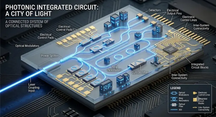
An comprehensive isometric 3D infographic illustration from an angled top-down perspective, depicting a 'photonic integrated circuit' built upon a multi-layered silicon platform conceptualized as an elaborate miniature "City of Light". A powerful, glowing blue laser beam enters from the left edge at a marked 'Laser Coupling Input' section. Inside the translucent chip material, a complex, interconnected network of extremely thin, glowing blue optical waveguides routes the light, function as microscopic city streets and avenues. The 'city' is organized into functional zones and components with clear labels: 'Optical Modulators' with complex structures and adjacent 'Electrical Control Pads' with trace connections, distinct circular and rectangular 'Ring Resonators', and a multi-stage 'Optical Filter'. Waveguides branch at a 'Power Splitter' into multiple paths, loop, and recombine, connecting these structures to 'Detectors' linked to 'Electrical Output Pins'. Adjacent to the optical pathways, complex gold-colored 'Electronic Control Lines' and small 'Integrated Circuit Blocks' are seamlessly integrated on the same multi-layered silicon-on-insulator (SOI) platform, showing interconnections to the photonic devices, and labeled 'Inter-System Connectivity'. Functional components on the chip glow internally, and small stylized buildings resemble the functional optical structures. A legend defines icons for component types, the SOI layer structure, and inter-system connectivity. The entire scene shows a large complex chip on a textured dark circuit board with additional surface-mount electronic components. Text titles read: 'PHOTONIC INTEGRATED CIRCUIT: A CITY OF LIGHT' and 'A CONNECTED SYSTEM OF OPTICAL STRUCTURES'.
The Evolutionary Path: History, Indirect Bandgap Bottlenecks, and Foundry Milestones
The migration of optical systems onto silicon wafers modified the chip manufacturing ecosystem by turning passive silicon layers into sub-micron light distribution networks.
The Historical Journey
The origins of silicon-based wave routing emerged in the late 1980s when Richard Soref mapped out the foundational electro-optic equations governing refractive index shifts in elemental silicon. During the 1990s, the introduction of standard silicon-on-insulator (SOI) crystal wafers provided the refractive contrast needed to guide optical modes around tight corners without immense radiation losses. By 2004, active commercial foundries demonstrated high-speed silicon modulators reaching gigahertz speeds, establishing that industrial complementary metal-oxide-semiconductor (CMOS) fabrication facilities could mass-produce complex optical systems alongside traditional microchips.
Contemporary Technical Bottlenecks
The primary material challenge limiting standard silicon crystal architectures is its native indirect electronic bandgap. Because silicon electrons must change their momentum vector to relax across the energy gap, they release energy as acoustic heat vibrations rather than emitting useful photons. This fundamental boundary means that silicon cannot naturally serve as an efficient active laser source. To address this limitation, hardware designers mount external semiconductor lasers adjacent to the wafer or use plasma-assisted bonding to add native direct-bandgap indium-phosphide crystals directly onto the silicon routing layer.
Future Horizons: Co-Packaged Data Interconnects and Thin-Film Lithium Niobate
Modern packaging technology is expanding silicon architectures past communication links into micro-processing centers:
- Co-Packaged Optical Input/Output Cores: To eliminate the high power demands and clock latency introduced by old metal circuit connections, engineers are mounting silicon photonic chips inside the same protective casing as main GPU and artificial intelligence processors. This layout transfers high-volume data streams between logic blocks and memory arrays using low-power light beams.
- Lithium Niobate Heterogeneous Wafers: To push electro-optic modulation speeds past classical silicon carrier limits, foundries are depositing thin layers of crystalline lithium niobate over silicon-on-insulator substrates. This hybrid architecture combines the high-speed phase control of specialized crystals with the scalability and compact core footprint of traditional silicon chip lines.
Silicon Photonics in One Simple Comparison
Silicon photonics can be understood by comparing it with ordinary electronics and traditional optical systems.
| System | Main Signal | Main Pathway | Strength | Limitation |
|---|---|---|---|---|
| Electronic circuit | Electrical current or voltage | Metal wires and transistors | Excellent for logic, memory, control, and computation | High-speed data movement can face power and bandwidth limits |
| Traditional optical system | Light beam | Lenses, mirrors, fibres, filters, and free-space paths | Excellent for imaging, measurement, and high-quality optical control | Can be bulky, alignment-sensitive, and difficult to scale |
| Silicon photonic circuit | Guided light signal | Silicon-based waveguides and photonic devices | Compact, scalable, and compatible with chip-based integration | Requires careful design, coupling, packaging, and material integration |
The goal of silicon photonics is not to replace every electronic or optical system. Its goal is to use light where light has clear advantages, especially in high-speed communication, optical interconnects, sensing, and compact photonic systems.
The Silicon-on-Insulator Platform
Many silicon photonic devices are built on a silicon-on-insulator platform, often shortened to SOI. In this structure, a thin silicon layer sits above an insulating silicon dioxide layer. The high refractive index of silicon compared with silicon dioxide helps confine light inside narrow silicon waveguides.
This structure is useful because it allows light to be guided in very small paths. Compact waveguides can bend, split, recombine, and pass through active devices. This makes it possible to build complex photonic integrated circuits on a chip.
Students should remember that a waveguide is not just a tiny pipe. It supports optical modes, and those modes depend on wavelength, geometry, refractive index, polarisation, and fabrication quality.
Core Building Blocks of Silicon Photonics
A silicon photonic chip is built from smaller photonic components. Each component performs one optical function. Together, they form a system for routing and processing light.
| Building Block | Main Function | Student-Friendly Meaning |
|---|---|---|
| Silicon waveguide | Guides light along a chip path | Optical wiring |
| Splitter | Divides one light signal into two or more paths | A branch in the light road |
| Coupler | Transfers light between fibres, waveguides, or devices | A connection point for light |
| Modulator | Changes intensity, phase, or another property of light | A device that writes information onto light |
| Ring resonator | Selects or changes specific wavelengths | A tiny loop that responds to selected colours |
| Photodetector | Converts light into an electrical signal | The optical receiver |
| Thermal tuner | Adjusts optical behaviour by changing temperature | A fine control knob |
| Fibre interface | Couples chip light into or out of an optical fibre | The doorway between chip and fibre |
Silicon Waveguides: Optical Wiring on a Chip
Silicon waveguides are among the most important parts of silicon photonics. They guide infrared light through patterned paths on a chip. Because silicon can confine light strongly, waveguides can be narrow and compact.
This compactness is useful, but it also creates design challenges. Small waveguides can be sensitive to roughness, fabrication variation, bending loss, polarisation effects, and coupling difficulty. A waveguide that is too tightly bent may lose light. A waveguide that is poorly matched to a fibre may waste optical power at the input or output.
The design of silicon waveguides therefore involves careful balance. Engineers want strong confinement, low loss, compact size, stable behaviour, and manufacturable geometry.
Modulators in Silicon Photonics
A silicon photonic modulator changes the optical signal so that information can be carried by light. In many systems, an electrical data signal controls the modulator, and the modulator changes the light’s intensity or phase.
Silicon modulators often use changes in free-carrier concentration to change optical properties. In simple terms, adding or removing mobile charge carriers in the silicon changes how light travels through the device. This allows the optical wave to be controlled by an electrical signal.
Modulators are central to optical communication because a steady beam of light does not automatically carry information. A modulator writes the message onto the light.
Ring Resonators in Silicon Photonics
A ring resonator is a small looped waveguide placed near a straight waveguide. At certain wavelengths, light couples into the ring and circulates strongly. This resonance behaviour can be used for filtering, modulation, switching, sensing, and wavelength selection.
Ring resonators are attractive because they can be compact. They can also interact strongly with specific wavelengths. However, they can be sensitive to temperature and fabrication variation. A small change in refractive index or geometry can shift the resonance wavelength.
This makes ring resonators a useful example of a wider design truth in silicon photonics: compactness is powerful, but it often comes with sensitivity.
Photodetectors and Germanium Integration
A photodetector converts incoming light into an electrical signal. Silicon itself is not ideal for detecting some important infrared communication wavelengths. For this reason, silicon photonic platforms often integrate detector materials such as germanium.
Germanium can respond usefully to important near-infrared wavelengths used in optical communication. When integrated with silicon waveguides, it allows a chip to receive optical signals and convert them into electrical currents.
This is a good example of practical engineering. A silicon photonic system does not have to use only silicon for every function. It may use silicon where silicon is strong and add other materials where they are needed.
The Light Source Challenge
One of the important challenges in silicon photonics is the light source. Silicon is not naturally an efficient laser material. This is because of its electronic band structure, which makes direct light emission inefficient compared with materials such as indium phosphide or gallium arsenide.
As a result, many silicon photonic systems use external lasers or integrate laser materials with silicon through hybrid or heterogeneous methods. The laser may sit off-chip and send light into the silicon photonic chip, or it may be attached to the silicon platform using specialised integration techniques.
Students should see this not as a failure of silicon photonics, but as a design reality. Modern technology often succeeds by combining materials intelligently rather than expecting one material to do everything.
Fibre-to-Chip Coupling
A silicon photonic chip often needs to connect to optical fibres. This is not trivial. Optical fibres have mode sizes that are much larger than many silicon waveguide modes. If the light is not transferred carefully, much of the optical power can be lost.
Engineers use structures such as grating couplers, edge couplers, tapers, and specialised packaging methods to improve fibre-to-chip coupling. The goal is to transfer light efficiently between the outside world and the tiny waveguides on the chip.
This reminds students that the chip is only one part of the system. Packaging, alignment, temperature control, and optical interfaces are all important.
Why Silicon Photonics Matters for Data Centres
Data centres move enormous amounts of information between servers, processors, storage units, and network switches. As data rates grow, electrical connections can face challenges related to bandwidth, power consumption, heat, and signal integrity.
Silicon photonics can help by using light for high-speed data movement. Optical signals can carry large amounts of information, especially when multiple wavelengths are used. Silicon photonic transmitters, receivers, modulators, and wavelength-handling structures can support compact optical links for data-centre infrastructure.
This is one reason silicon photonics is strongly connected with Cloud Computing, and Data Science and Analytics.
Silicon Photonics and Optical Interconnects
An interconnect is a connection that moves data between parts of a system. Traditional electronic interconnects use electrical signals. Optical interconnects use light. Silicon photonics is important because it offers a path toward compact optical interconnects that can be integrated with electronic systems.
Optical interconnects are especially attractive when large amounts of data must travel quickly and efficiently. In future systems, optical links may connect servers, boards, chip packages, processor clusters, memory systems, or specialised accelerators.
The deeper idea is that computing is not only limited by how fast a processor can calculate. It is also limited by how fast data can move. Silicon photonics addresses the movement of information.
Silicon Photonics in Sensing
Silicon photonics is not limited to communication. It can also support sensing. A guided optical wave may respond to changes in temperature, strain, pressure, chemical concentration, biological samples, gases, or refractive index near the waveguide.
Ring resonators, interferometers, and waveguide sensors can be designed so that small environmental changes produce measurable optical changes. These changes may appear as shifts in wavelength, phase, intensity, or resonance condition.
This makes silicon photonics useful for compact sensing systems, including environmental monitoring, biomedical diagnostics, industrial measurement, and lab-on-chip technologies.
Silicon Photonics and Computing
Silicon photonics is often discussed in connection with future computing. The most immediate role is usually optical communication: moving data faster and more efficiently between computing components. This includes optical interconnects inside data centres and advanced computing systems.
Some researchers also explore photonic approaches to computation, signal processing, Artificial Intelligence hardware, and quantum information. These areas are still developing and should be understood carefully. Photonics has strengths, but it does not automatically replace all electronic computing.
A balanced view is best: electronics remains powerful for logic and memory, while photonics is especially strong for high-bandwidth data movement, wavelength-based parallelism, sensing, and some specialised forms of signal processing.
Silicon Photonics Versus General Photonic Integrated Circuits
Silicon photonics is one important type of photonic integrated circuit platform. It should not be confused with all photonic integrated circuits. PICs can also be made using indium phosphide, silicon nitride, lithium niobate, silica, polymers, and other material systems.
| Topic | Photonic Integrated Circuits | Silicon Photonics |
|---|---|---|
| Main meaning | Any chip that integrates photonic components | A silicon-based platform for integrated photonics |
| Material scope | Many possible material platforms | Uses silicon-based structures, often with added materials |
| Typical strength | Depends on platform and application | Compact waveguides and semiconductor-manufacturing relevance |
| Light source issue | Some platforms integrate lasers more naturally | Efficient laser integration is a major design challenge |
| Common applications | Communication, sensing, quantum photonics, imaging, signal processing | Data communication, optical interconnects, sensing, chip-scale photonic systems |
The relationship is simple: silicon photonics is a major branch of photonic integrated circuits, but not the only branch.
Strengths and Challenges of Silicon Photonics
Silicon photonics is powerful because it combines compact optics with semiconductor-style thinking. However, every strength comes with design challenges.
| Strength | Why It Helps | Related Challenge |
|---|---|---|
| Compact waveguides | Allow dense photonic circuits | Can increase sensitivity to fabrication errors and roughness |
| Semiconductor manufacturing relevance | Supports scalability and repeatability | Photonic packaging remains complex |
| Good infrared guiding | Useful for optical communication wavelengths | Not equally suitable for all wavelength ranges |
| Electronic integration | Allows close control and signal processing | Thermal and electrical effects must be managed |
| Wavelength multiplexing | Can move many channels through one optical path | Requires filters, tuning, stability, and low crosstalk |
| Platform flexibility | Can combine silicon with germanium, silicon nitride, or laser materials | Integration steps add design and manufacturing complexity |
Case Studies: Silicon Photonics in Real Systems
Case Study 1: Optical Transceivers
An optical transceiver converts electrical data into optical signals and then converts received optical signals back into electrical data. Silicon photonics can help integrate modulators, waveguides, couplers, filters, and detectors into a compact transceiver platform.
This case study shows why silicon photonics matters for high-speed communication. It helps turn optical communication from a set of separate components into a compact module that can be used in data centres and network systems.
Case Study 2: Wavelength-Division Multiplexing
A single optical fibre or waveguide can carry multiple wavelength channels at the same time. Silicon photonic filters, resonators, and multiplexers can help combine or separate these channels.
This case study shows how silicon photonics uses the wave nature of light. Different wavelengths can behave like different lanes on the same highway, increasing the amount of information that can be carried.
Case Study 3: Ring-Resonator Sensors
A silicon ring resonator can be designed so that its resonance wavelength changes when the surrounding environment changes. If a biological sample, gas, liquid, or temperature change affects the optical environment, the resonator response can shift.
This case study shows how a small waveguide structure can become a sensitive measurement tool. Silicon photonics is therefore not only about communication; it can also support compact sensing.
Case Study 4: Optical I/O for Advanced Computing
As computing systems grow, moving data into and out of processors can become a major bottleneck. Silicon photonics can support optical input and output links that move data using light rather than only electrical signals.
This case study shows why silicon photonics is important for future computing infrastructure. The challenge is not only calculation, but communication between parts of the computing system.
Connections with Wider Physics and Technology
Silicon photonics connects physics, optics, electronics, semiconductor manufacturing, communication systems, and computing. These related pages help students see the wider learning map.
Light and Optics
Silicon photonics belongs to the wider study of how light travels, reflects, refracts, interferes, diffracts, and interacts with matter.Wave Optics
Waveguides, modes, phase, interference, resonance, and wavelength selection are central to silicon photonic design.Fiber Optics
Silicon photonic chips often connect to optical fibres, which carry light signals across rooms, buildings, cities, and continents.Laser Optics
Lasers provide the organised light needed by many silicon photonic communication and sensing systems.Electrical and Electronic Engineering
Silicon photonics works closely with electronic drivers, receivers, amplifiers, control circuits, packaging, and semiconductor devices.Chemical Material Engineering
Developing silicon-on-insulator structures demands high-purity crystalline chemical processing to ensure zero-loss propagation interfaces.Learning Pathway Within Photonics
This page builds on photon energy, photonic devices, waveguides, modulators, and photonic integrated circuits. It prepares students for system-level applications in communication and computing.
Photons and Photon Energy
Understand photons, wavelength, frequency, photon energy, absorption, emission, and energy matching in photonic materials.LEDs, Lasers, and Photodetectors
Learn how photonic devices emit, amplify, detect, and convert light signals.Optical Modulators and Waveguides
See how light signals are guided, switched, shaped, encoded, and routed through optical systems.Photonic Integrated Circuits
Discover how waveguides, modulators, detectors, filters, resonators, and optical components can be combined on compact chips.Silicon Photonics
Current page. Explore how silicon-based platforms guide, modulate, detect, and process light for communication, sensing, and optical interconnects.Photonics in Communication and Computing
Understand how photonic systems support fibre networks, data centres, optical interconnects, and future computing systems.Quick Check: Silicon Photonics
Quick Check: Silicon Photonics
Q1. What is silicon photonics?
Silicon photonics is the use of silicon-based chip technology to guide, control, modulate, detect, and process light in compact photonic systems.
Q2. Why is silicon attractive for photonics?
Silicon is attractive because it is already central to semiconductor manufacturing and can guide important infrared communication wavelengths in compact waveguides.
Q3. Why is making efficient lasers on silicon difficult?
Silicon is not naturally an efficient light-emitting material. Many silicon photonic systems therefore use external lasers or integrate other light-emitting materials with the silicon platform.
Q4. Why are germanium detectors often useful in silicon photonics?
Germanium can detect important near-infrared communication wavelengths more effectively than silicon, so it is often integrated with silicon waveguides for photodetection.
Common Misunderstandings About Silicon Photonics
Misunderstanding 1: Silicon Photonics Means Everything Is Made Only from Silicon
Silicon is the platform, but many systems combine silicon with other materials. Germanium may be used for detectors, III-V materials may be used for light sources, and silicon nitride may be used for low-loss waveguides. Silicon photonics often succeeds through material teamwork.
Misunderstanding 2: Silicon Photonics Is Just Smaller Fibre Optics
Both fibre optics and silicon photonics guide light, but they operate in different physical and engineering settings. Fibre optics guides light over long distances through fibres. Silicon photonics guides and controls light in tiny chip-scale structures that may interact closely with electronics.
Misunderstanding 3: Photonics Will Replace Electronics Completely
Photonics has major strengths, especially in communication and high-bandwidth data movement. However, electronics remains excellent for logic, memory, switching, control, and many forms of computation. Future systems are likely to combine both.
Misunderstanding 4: A Good Chip Design Is Enough
A silicon photonic chip also needs good packaging, fibre coupling, laser integration, electronic drivers, thermal control, testing, and system design. The full module matters, not just the patterned chip.
Key Terms
- Edge coupler
- A coupling structure that transfers light through the edge of a chip into or out of a waveguide.
- Germanium photodetector
- A detector material often integrated with silicon photonics to detect important near-infrared wavelengths.
- Grating coupler
- A patterned structure that helps couple light between an optical fibre and a chip waveguide.
- Heterogeneous integration
- A more advanced integration approach that combines different material systems within a shared photonic or electronic platform.
- Hybrid integration
- A method of combining different materials or devices so that each contributes useful properties.
- Modulator
- A device that changes an optical signal, often to encode information onto light.
- Optical interconnect
- A connection that uses light to transfer data between devices, boards, chips, or systems.
- Photonic I/O
- Optical input and output used to move data into and out of computing or communication systems.
- Ring resonator
- A looped waveguide that interacts strongly with selected wavelengths and can be used for filtering, modulation, sensing, or switching.
- Silicon photonics
- A technology field that uses silicon-based platforms to guide, control, modulate, detect, and process light on chips.
- Silicon waveguide
- A patterned silicon structure that confines and guides light on a chip.
- Silicon-on-insulator
- A common platform in which a thin silicon layer sits above an insulating silicon dioxide layer.
- Thermal tuning
- Changing the temperature of a photonic device to adjust its optical behaviour.
- Wavelength-division multiplexing
- A technique that sends multiple wavelength channels through the same optical path.
Review Questions
- What is silicon photonics?Answer: Silicon photonics is the use of silicon-based chip technology to guide, control, modulate, detect, and process light.
- Why is silicon useful as a photonic platform?Answer: Silicon is useful because it is central to semiconductor manufacturing and can guide important infrared wavelengths in compact chip-scale waveguides.
- What is the role of a silicon waveguide?Answer: A silicon waveguide confines and directs light along a chosen path on a chip.
- Why are modulators important in silicon photonics?Answer: Modulators change optical signals so that information can be encoded onto light.
- Why is laser integration a challenge in silicon photonics?Answer: Silicon is not naturally an efficient light-emitting material, so silicon photonic systems often use external lasers or integrate other light-emitting materials.
- Why does silicon photonics matter for data centres?Answer: Data centres need to move very large amounts of information quickly and efficiently. Silicon photonics can support compact high-speed optical links for this purpose.
Thought-Provoking Questions
- Why is silicon photonics a bridge between electronics and optics?Answer: It uses chip-based silicon technology from electronics while guiding and controlling light using optical principles. This allows electronic and photonic systems to work closely together.
- Why might data movement become as important as data processing?Answer: A processor may calculate quickly, but performance can still be limited if data cannot move efficiently between chips, memory, servers, or systems. Silicon photonics addresses this movement problem.
- Why does silicon photonics often require more than one material?Answer: Silicon is excellent for some functions, such as compact waveguiding, but other materials may be better for light emission, detection, low-loss guiding, or high-speed modulation. Combining materials allows stronger systems.
- How does silicon photonics show that engineering is often about trade-offs?Answer: Engineers must balance size, loss, speed, power, coupling efficiency, thermal stability, fabrication limits, packaging, and cost. A design that improves one feature may make another feature harder.
Comprehensive Numerical Problems with Solutions
- Light travels through a silicon photonic waveguide with an effective refractive index n = 2.4. Estimate the speed of light in the waveguide using the standard phase velocity equation.Solution:Apply the refractive phase velocity formula:$$v = \frac{c}{n}$$Substitute the values ($c = 3.00 \times 10^8\text{ m/s}$ and $n = 2.4$):$$v = \frac{3.00 \times 10^8\text{ m/s}}{2.4} = 1.25 \times 10^8\text{ m/s}$$Answer: The wave velocity through the silicon channel track equals exactly 1.25 × 10⁸ m/s.
- A silicon photonic waveguide is 2.0 cm long. Light travels through it at a speed of 1.5 × 10⁸ m/s. Estimate the total path travel time.Solution:1. Convert the physical channel segment metric from centimeters to meters:$$d = 2.0\text{ cm} = 2.0 \times 10^{-2}\text{ m} = 0.020\text{ m}$$2. Apply the velocity transit duration formula:$$t = \frac{d}{v}$$3. Substitute parameters straight into the equation:$$t = \frac{0.020\text{ m}}{1.5 \times 10^8\text{ m/s}} \approx 1.3333 \times 10^{-10}\text{ s}$$Convert units to nanoseconds (ns), where 1 ns = 10−9 s:$$t \approx 0.1333\text{ ns}$$Answer: The total path transit time is approximately 0.13 ns.
- A fibre-to-chip coupler interface receives 10 mW of input optical power, but only 7.0 mW successfully enters the silicon waveguide core. What percentage of the power is coupled?Solution:Calculate the quotient of captured power over launch power:$$\text{Coupling Efficiency} = \frac{P_{\text{waveguide}}}{P_{\text{input}}}$$$$\text{Coupling Efficiency} = \frac{7.0\text{ mW}}{10\text{ mW}} = 0.70$$Convert the raw decimal fraction into a percentage factor:$$\text{Percentage} = 0.70 \times 100\% = 70\%$$Answer: Exactly 70% of the input power couples successfully into the waveguide.
- A wavelength-division multiplexing link uses 4 color channels. If each unique channel carries a data rate of 50 Gbit s−1, calculate the total combined throughput.Solution:The total capacity is the product of parallel color tracks and lane line rates:$$\text{Total Data Rate} = \text{Channels} \times \text{Channel Rate}$$$$\text{Total Data Rate} = 4 \times 50\text{ Gbit s}^{-1} = 200\text{ Gbit s}^{-1}$$Answer: The complete aggregate link data rate equals exactly 200 Gbit s−1.
- A integrated germanium detector produces 1.2 mA of photocurrent when receiving an input optical power level of 2.0 mW. Estimate its responsivity using the quotient formula.Solution:Convert both metric parameters to standard base scientific units ($I = 1.2 \times 10^{-3}\text{ A}$ and $P = 2.0 \times 10^{-3}\text{ W}$):$$R = \frac{I}{P}$$$$R = \frac{1.2 \times 10^{-3}\text{ A}}{2.0 \times 10^{-3}\text{ W}} = 0.60\text{ A/W}$$Answer: The photodetector responsivity scales to exactly 0.60 A/W.
External References for Further Reading
The following references provide useful background for students who want to read beyond this introductory page.
- RP Photonics Encyclopedia: Silicon Photonics — A detailed overview of silicon photonics, including silicon waveguides, modulators, detectors, light sources, and applications.
- MIT OpenCourseWare: Fundamentals of Photonics Lecture Notes — Lecture materials covering integrated optics, waveguides, optical fibres, resonators, and related photonics foundations.
- imec: Silicon Photonics Foundry Services — An industry-facing overview of silicon photonics platforms, integration options, and application areas.
- Intel: Silicon Photonics — A technology overview showing how silicon photonics is used in high-speed optical connectivity.
Why This Topic Matters
Silicon photonics matters because modern technology increasingly depends on moving information quickly, efficiently, and reliably. Electronics remains powerful for logic and control, but optical links can help carry large amounts of data across systems. Silicon photonics offers one path toward compact optical communication and interconnection using chip-based platforms.
For students, this topic is important because it brings together many earlier ideas: photon energy, waveguides, optical modulation, photodetection, semiconductor materials, fibre communication, photonic integrated circuits, and computing infrastructure.
The deeper lesson is that future technology may not belong to electronics alone or optics alone. It may depend on carefully designed partnerships between electrons and photons.
Summary
Silicon photonics uses silicon-based chip platforms to guide, modulate, detect, and process light. It is especially important for optical communication, optical interconnects, data centres, sensing, and compact photonic systems.
Silicon waveguides can confine infrared light strongly, enabling compact photonic circuits. However, silicon is not ideal for every function. Light sources, detectors, low-loss guiding, coupling, and packaging often require additional materials or careful engineering.
Students who understand silicon photonics are ready to study how photonics supports communication and computing, especially in systems where moving data efficiently becomes as important as processing data.
Reflection Question
If silicon helped make electronics small, affordable, and powerful, how might silicon photonics change the way future systems move information using light?