
Photonic integrated circuits are compact systems that guide, control, split, combine, filter, modulate, and detect light on a chip. Just as electronic integrated circuits combine many electronic components on a small semiconductor platform, photonic integrated circuits combine many optical functions into a much smaller and more stable form than traditional bench-top optical systems.
This page introduces Photonic Integrated Circuits in a student-friendly way. It belongs to the wider Photonics cluster, where students can also study Photons and Photon Energy, LEDs, Lasers, and Photodetectors, Optical Modulators and Waveguides, Silicon Photonics, and Photonics in Communication and Computing.
What Photonic Integrated Circuits Really Are
A photonic integrated circuit, often shortened to PIC, is a chip that uses light instead of only electrical current to perform useful functions. It may contain waveguides, splitters, couplers, resonators, modulators, filters, detectors, and sometimes light sources. These components work together to move and process optical signals.
A simple way to understand a photonic integrated circuit is to compare it with a miniature optical laboratory. In a traditional laboratory, light may travel through lenses, mirrors, beam splitters, filters, modulators, and detectors placed on an optical table. In a PIC, many of those functions are compressed into tiny structures on a chip.
The most important idea is not merely small size. The deeper idea is integration. By placing many optical functions close together, engineers can build systems that are more compact, more stable, more scalable, and easier to connect with electronics.
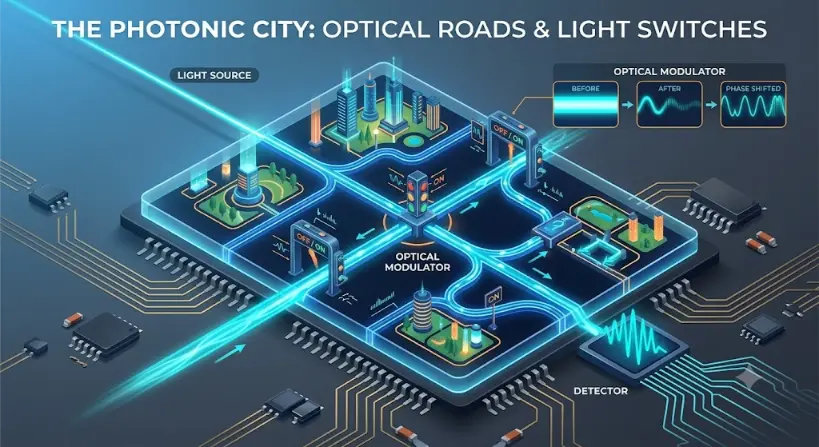
The image is a detailed 3D isometric scientific infographic comparing an integrated photonic chip to a miniature city layout. At the top left, a powerful blue laser beam labeled "Light Source" enters the main chip. The chip itself is a square platform divided into grid sectors featuring miniature futuristic buildings and parks. The beam splits and travels through a network of glowing, transparent channel pathways that represent optical waveguides acting as city streets. At a key intersection, a central pillar stylized like a traffic light is labeled "Optical Modulator," alongside archway gates labeled "OFF/ON." These gates signify modulation points that manipulate the beam. An inset diagram on the top right shows a step-by-step waveform transformation labeled "OPTICAL MODULATOR," depicting a constant stream ("Before") changing into a modulating wave ("After") and then a modified wavelength state ("Phase Shifted"). At the bottom right, the final structured light wave exits the city grid and hits a processing unit labeled "Detector," which translates the light into complex electronic signals traveling down copper-toned circuit paths.The Evolutionary Path: History, System Barriers, and Foundry Paradigms
The shift from discrete free-space lenses to single-substrate wave systems redefined the physical boundaries of data transmission speed and structural alignment stability.
The Historical Journey
The concept of planar integrated optics was introduced in 1969 by Stewart Miller at Bell Labs, who proposed using lithographic techniques to form networks of miniature waveguides and filters on small glass or semiconductor hosts. Throughout the 1970s and 1980s, active material platforms based on Indium Phosphide (InP) emerged to fulfill Miller’s vision, demonstrating that light generation, modulation, and routing could occur on a single crystal block.
By the early 2000s, commercial foundries successfully coupled optical waveguides with large-scale silicon processing lines, transforming PICs from specialized optical physics components into standard infrastructure chips for massive global cloud networks.
Contemporary Technical Barriers
The primary technical challenge in advanced photonic chip architecture is minimizing insertion losses while maximizing the internal device count. Unlike electrons, which flow smoothly around tight copper traces, photons scatter heavily when encountering any sidewall roughness left behind by chemical etching processes.
Furthermore, coupling a standard single-mode silica fiber core (roughly 9 microns wide) to a sub-micron silicon waveguide track creates a severe physical mismatch. This geometric barrier requires the fabrication of specialized micro-lenses or precisely tapered grating structures to prevent severe optical power loss during fiber-to-chip connection.
Future Paradigms: Heterogeneous Substrates and Automated Packaging
The horizon of monolithic system scaling relies on marrying different crystalline properties within highly automated micro-assemblies:
- Heterogeneous III-V Plasma Bonding: Because native Silicon possesses an indirect band gap that prevents efficient photon generation, foundries are molecularly bonding thin sheets of Indium Phosphide directly onto silicon-on-insulator (SOI) wafers. This technique allows lasers, amplifiers, and high-speed modulators to share the same compact floor space as ultra-low-loss silicon pathways.
- Passive Machine-Vision Alignment In traditional packaging setups, micro-positioning individual fiber connections to sub-micron alignment tolerances requires active laser testing, which limits production throughput. Modern cleanrooms are transitioning to passive automated flip-chip bonders that use precision physical mechanical stops and computer-vision tracking to snap optoelectronic interfaces together cleanly in seconds.
Why Integration Matters
Traditional optical systems can be powerful, but they may require careful alignment, large spaces, many separate components, and delicate mechanical stability. A photonic integrated circuit reduces these difficulties by placing optical functions into fixed chip-scale structures.
Integration matters because modern technology increasingly needs high speed, compact size, low power consumption, repeatable manufacturing, and reliable data movement. Photonic integrated circuits help meet these needs by allowing light signals to be routed and controlled in compact platforms.
| Traditional Optical System | Photonic Integrated Circuit | Why It Matters |
|---|---|---|
| Separate lenses, mirrors, fibres, and detectors | Many optical functions on one chip | Reduces size and alignment difficulty |
| Often sensitive to vibration and temperature | More mechanically stable once fabricated | Improves reliability |
| Harder to mass-produce exactly | Can use semiconductor-style fabrication methods | Supports scaling and repeatability |
| Large optical pathways | Tiny waveguide pathways | Allows compact communication and sensing systems |
| Separate optical and electronic modules | Can be closely connected with electronics | Supports high-speed optoelectronic systems |
From Electronic Circuits to Photonic Circuits
Electronic integrated circuits guide and process electrical signals using conductors, transistors, resistors, capacitors, and other electronic elements. Photonic integrated circuits guide and process optical signals using waveguides, modulators, couplers, resonators, filters, and detectors.
The comparison is useful, but it should not be pushed too far. Electrons and photons behave differently. Electrons carry charge and interact strongly with each other and with circuit materials. Photons carry electromagnetic energy and can move very quickly through transparent structures, but they are harder to stop, store, and switch directly at very small scales.
This is why future systems often combine both worlds. Electronics remains excellent for logic, memory, control, and general computation. Photonics is especially powerful for high-speed communication, sensing, optical interconnects, wavelength-based multiplexing, and signal transmission with low loss over distance.
Main Components of a Photonic Integrated Circuit
A photonic integrated circuit is built from smaller functional blocks. Different chips may contain different combinations of these blocks depending on the application.
| Component | Main Function | Student-Friendly Meaning |
|---|---|---|
| Waveguide | Guides light along a chosen path | Optical wiring on the chip |
| Splitter | Divides one optical signal into two or more paths | A branching road for light |
| Coupler | Transfers light between nearby waveguides or between fibre and chip | A controlled light connection |
| Modulator | Changes intensity, phase, or another property of light | A device that writes information onto light |
| Ring resonator | Selects or modifies specific wavelengths | A tiny loop that responds strongly to certain colours |
| Filter | Selects part of the optical spectrum | A wavelength selector |
| Photodetector | Converts light into an electrical signal | The chip’s optical receiver |
| Light source | Provides optical input | The beginning of the light signal |
Waveguides as Optical Wiring
Waveguides are the basic pathways of a photonic integrated circuit. They confine light and guide it across the chip. Without waveguides, light would spread out and be difficult to control in such a small space.
A waveguide usually has a core region with a suitable refractive index contrast relative to its surroundings. This contrast helps confine the optical mode. The shape, width, height, material, wavelength, and bending radius all affect how light travels through the guide.
Students can study waveguide behaviour more fully in Optical Modulators and Waveguides.
Splitters, Couplers, and Interference
Photonic chips often need to divide and recombine optical signals. A splitter can send one optical input into two or more paths. A coupler can transfer light between nearby waveguides. These components allow a chip to distribute light, compare signals, form interferometers, or connect different parts of a circuit.
Interference is especially important. When two light waves recombine, their relative phase affects whether they strengthen or weaken each other. This principle appears in many photonic devices, including Mach-Zehnder interferometers, modulators, filters, sensors, and coherent communication systems.
This means a photonic integrated circuit is not only a set of tiny light pipes. It is a carefully designed wave system where phase, path length, coupling, and wavelength all matter.
Modulators: Writing Information onto Light
A modulator changes a property of the light signal. It may change intensity, phase, polarisation, frequency, or timing. In many communication systems, the modulator is the component that encodes data onto an optical carrier.
For example, a modulator may make the light stronger or weaker to represent information. More advanced systems may use phase or amplitude changes to carry more information per symbol. On photonic chips, modulators allow optical data to be created and controlled at high speed.
The modulator is one of the strongest examples of how photonics and electronics work together. An electrical signal can control the optical signal, allowing electronic data to be carried by light.
Ring Resonators and Filters
A ring resonator is a tiny looped waveguide placed close to another waveguide. At certain wavelengths, light couples strongly into the ring and circulates. At other wavelengths, the interaction is weaker. This makes ring resonators useful for filtering, wavelength selection, modulation, sensing, and signal routing.
The key idea is resonance. A ring supports strong circulating light only when the optical path fits the wave condition. Changing the temperature, refractive index, or geometry can shift the resonance condition. This makes ring resonators powerful but also sensitive.
Filters based on resonators or interference can separate wavelengths, clean signals, select channels, and support wavelength-division multiplexing. This is important because optical communication systems often use many wavelengths at the same time.
Photodetectors on Photonic Chips
A photodetector converts incoming light into an electrical signal. On a photonic integrated circuit, detectors may be placed at output ports or at monitoring points inside the circuit. They allow the system to read signals, measure power, monitor performance, or convert optical data back into electronics.
Detector material matters because photon energy must match the detector’s response. For some platforms, the best detector material is not the same as the best waveguide material. For example, some silicon photonics systems use germanium detectors because germanium is useful for detecting important infrared communication wavelengths.
Students can connect this section with LEDs, Lasers, and Photodetectors.
Light Sources and the Integration Challenge
A photonic integrated circuit needs light. The light may come from an external laser coupled into the chip, or from a light source integrated directly or indirectly with the platform. Integrating efficient light sources can be difficult, especially on silicon-based platforms.
This challenge exists because not all materials are good at emitting light. Some semiconductor materials are excellent for electronics and waveguides but poor as direct light emitters. Other materials are better for lasers but harder to integrate with standard semiconductor manufacturing.
As a result, photonic integrated circuits may use several approaches: external lasers, hybrid integration, heterogeneous integration, bonded materials, or separate laser modules connected to the chip. The best choice depends on cost, performance, wavelength, reliability, and system design.
Materials Used in Photonic Integrated Circuits
Different material platforms are used for photonic integrated circuits. Each material has strengths and limits. The right platform depends on wavelength range, optical loss, device size, fabrication method, modulation speed, detector integration, and application.
| Material Platform | Typical Strength | Common Challenge | Example Uses |
|---|---|---|---|
| Silicon photonics | Compact waveguides and compatibility with semiconductor manufacturing | Efficient on-chip light generation is difficult | Data communication, sensing, optical interconnects |
| Silicon nitride | Low optical loss and broad wavelength usefulness | May need integration with other active materials | Frequency combs, sensors, low-loss circuits |
| Indium phosphide | Good for active light sources and amplifiers | Different manufacturing ecosystem from silicon | Lasers, modulators, optical communication devices |
| Lithium niobate | Strong electro-optic modulation | Integration and fabrication can be more specialised | High-speed modulators, signal processing |
| Silica or glass | Low loss and stable passive optics | Larger device size compared with high-index platforms | Passive circuits, filters, interferometers |
| Polymers | Flexible material properties and possible low-cost processing | Thermal and long-term stability may need care | Sensors, modulators, specialised optical circuits |
Silicon Photonics and Photonic Integration
Silicon photonics is one of the most important approaches to photonic integration. It uses silicon-based structures to guide and process light, often at infrared wavelengths useful for communication. Silicon photonics is attractive because it can draw on ideas from semiconductor fabrication and electronic-chip manufacturing.
However, silicon photonics is not simply electronics with light added. The optical design must manage waveguide modes, bending loss, coupling, modulation, thermal effects, detector integration, and packaging. Light behaves differently from current in a wire.
The next page, Silicon Photonics, explores this platform in more detail.
Packaging and Coupling
A photonic chip does not work alone. It must be connected to light sources, optical fibres, electronic drivers, control circuits, power supplies, cooling systems, and external equipment. This makes packaging a major part of photonic integrated circuit design.
One important challenge is coupling light into and out of the chip. Optical fibres are much larger than many chip waveguides, so engineers must design couplers that transfer light efficiently. Poor coupling can waste optical power and reduce system performance.
Packaging also affects reliability, temperature stability, alignment, cost, and manufacturability. A brilliant chip design is not enough if it cannot be connected and used in a real system.
Loss, Speed, Power, and Footprint
Photonic integrated circuit design involves trade-offs. A smaller device may save space but become more sensitive to fabrication errors. A faster modulator may require more electrical power or introduce more optical loss. A tightly bent waveguide may help compactness but increase bending loss.
| Design Goal | Why It Matters | Possible Trade-Off |
|---|---|---|
| Low optical loss | Preserves signal strength | May require larger bends or smoother fabrication |
| High speed | Supports fast data transmission | May need stronger electrical drive or more complex design |
| Small footprint | Allows more components per chip | May increase thermal sensitivity or fabrication difficulty |
| Low power consumption | Reduces heat and operating cost | May limit modulation strength or tuning range |
| High coupling efficiency | Transfers light efficiently between fibre and chip | May require extra coupler structures and alignment care |
| Manufacturability | Allows repeatable large-scale production | May restrict design freedom or material choice |
Students should notice that photonic design is not about choosing the most impressive component. It is about balancing many physical and engineering requirements.
Applications of Photonic Integrated Circuits
Photonic integrated circuits are important because they can make optical systems smaller, faster, more scalable, and more practical. Their applications span communication, computing, sensing, imaging, measurement, quantum technology, and biomedical systems.
Optical Communication
PICs can support transmitters, receivers, wavelength multiplexing, modulation, filtering, and signal routing in fibre networks and data centres.Data Centres
Photonic chips can help move large amounts of data between servers, switches, processors, and memory systems with high bandwidth.Sensing
Integrated waveguides and resonators can detect changes in temperature, strain, chemicals, gases, biological samples, or refractive index.Lidar and Imaging
Photonic integration can help create compact optical systems for distance measurement, scanning, beam steering, and imaging.Quantum Photonics
Photonic chips can guide and interfere single photons, supporting research in quantum communication, quantum sensing, and quantum information.Biomedical Technology
Compact optical chips may support lab-on-chip sensing, medical diagnostics, imaging, and portable analytical instruments.Connections with Wider Physics and Technology
Photonic integrated circuits connect many areas of physics, engineering, and information technology. These related pages help students see the wider learning map.
Light and Optics
PICs belong to the wider study of how light travels, reflects, refracts, interferes, diffracts, and interacts with matter.Wave Optics
Interference, phase, guided modes, resonance, and wavelength behaviour are central to photonic chip design.Fiber Optics
PICs often connect to optical fibres, which carry light between chips, modules, buildings, cities, and continents.Laser Optics
Lasers provide the coherent light sources often used to feed photonic chips and optical communication systems.Electrical and Electronic Engineering
PICs often work with electronic drivers, control circuits, detectors, amplifiers, packaging, and signal-processing systems.Chemical Material Engineering
The stability of modern optical nodes depends on engineering semiconductor crystals with exact lattice parameters to limit signal attenuation.Learning Pathway Within Photonics
This page builds on photon energy, photonic devices, modulators, and waveguides. It prepares students for silicon photonics and for system-level applications in communication and computing.
Photons and Photon Energy
Understand photons, wavelength, frequency, photon energy, absorption, emission, and energy matching in photonic materials.LEDs, Lasers, and Photodetectors
Learn how photonic devices emit, amplify, detect, and convert light signals.Optical Modulators and Waveguides
See how light signals are guided, switched, shaped, encoded, and routed through optical systems.Photonic Integrated Circuits
Current page. Discover how waveguides, modulators, detectors, filters, resonators, and optical components can be combined on compact chips.Silicon Photonics
Explore how silicon-based platforms guide, modulate, detect, and process light for communication and sensing.Photonics in Communication and Computing
Understand how photonic systems support fibre networks, data centres, optical interconnects, and future computing systems.Quick Check: Photonic Integrated Circuits
Quick Check: Integrated Photonics
Q1. What is a photonic integrated circuit?
A photonic integrated circuit is a chip that combines optical components such as waveguides, modulators, splitters, filters, resonators, and detectors to guide and process light signals.
Q2. Why are waveguides important in PICs?
Waveguides act as optical wiring. They route light between different components on the chip.
Q3. Why is integrating a light source sometimes difficult?
Some chip materials are good for guiding light or making electronics but are not efficient light emitters. This means external lasers, hybrid integration, or other material combinations may be needed.
Q4. Why do PICs often combine photonics with electronics?
Electronics is useful for control, logic, memory, and signal processing, while photonics is useful for high-speed optical transmission, sensing, and interconnection. Combining them allows stronger systems.
Common Misunderstandings About Photonic Integrated Circuits
Misunderstanding 1: A Photonic Integrated Circuit Is Just a Smaller Optical Table
A PIC can replace some functions of a traditional optical table, but it is not simply a miniature version of separate lenses and mirrors. It uses guided modes, chip materials, integrated structures, lithographic patterns, couplers, resonators, and close links with electronics.
Misunderstanding 2: Photonic Chips Will Completely Replace Electronic Chips
Photonics is powerful, but it does not automatically replace electronics. Electronics remains highly effective for logic, memory, switching, and control. Photonic chips are most valuable where light offers clear advantages, such as high-speed communication, low-loss transmission, sensing, and optical interconnects.
Misunderstanding 3: Smaller Always Means Better
Smaller photonic devices can reduce footprint, but they may increase loss, thermal sensitivity, fabrication difficulty, and coupling challenges. Good PIC design balances size, performance, power, stability, cost, and manufacturability.
Misunderstanding 4: The Chip Alone Determines System Performance
The chip is important, but the full system also depends on packaging, fibre coupling, laser sources, electronic drivers, temperature control, detectors, power supply, and software control. A photonic chip must work as part of a complete system.
Key Terms
- Coupling loss
- Power loss that occurs when light is transferred inefficiently between fibres, waveguides, chips, or components.
- Heterogeneous integration
- A method of integrating different material systems so that each material contributes useful optical or electronic properties.
- Hybrid integration
- An approach that combines different materials or devices on the same photonic platform.
- Insertion loss
- The reduction in optical power caused by adding a component, connection, or device to an optical path.
- Optical coupler
- A structure that transfers light between waveguides, fibres, or chip regions.
- Optical modulator
- A device that changes a property of light, such as intensity or phase, to encode or control a signal.
- Optical interconnect
- A connection that uses light to transfer data between devices, boards, chips, servers, or systems.
- Optical splitter
- A component that divides one optical signal into two or more paths.
- Photodetector
- A device that converts incoming optical energy into an electrical signal.
- Photonic integrated circuit
- A chip that combines multiple optical or photonic components to guide, control, process, and detect light.
- Ring resonator
- A looped waveguide structure that interacts strongly with selected wavelengths.
- Silicon photonics
- A field that uses silicon-based platforms to guide, modulate, detect, and process light.
- Waveguide
- A structure that confines and directs light along a chosen path.
- Wavelength-division multiplexing
- A technique that sends multiple optical wavelength channels through the same fibre or optical path.
Review Questions
- What is a photonic integrated circuit?Answer: A photonic integrated circuit is a chip that combines multiple optical components such as waveguides, modulators, splitters, filters, resonators, and detectors to guide and process light.
- Why are waveguides central to PICs?Answer: Waveguides route light between components on the chip. They act like optical wiring.
- What does an optical modulator do in a PIC?Answer: It changes a property of light, such as intensity or phase, so that information can be encoded or the optical signal can be controlled.
- Why are ring resonators useful in integrated photonics?Answer: Ring resonators interact strongly with selected wavelengths, making them useful for filtering, modulation, sensing, and wavelength routing.
- Why is packaging important for photonic integrated circuits?Answer: Packaging connects the chip to fibres, lasers, detectors, electronics, cooling, power, and external systems. Poor packaging can reduce performance even if the chip design is good.
- Why do photonic integrated circuits often work together with electronics?Answer: Electronics provides control, logic, memory, and signal processing, while photonics provides high-speed optical transmission, sensing, and interconnection.
Thought-Provoking Questions
- Why is integration such a powerful idea in technology?Answer: Integration reduces size, improves stability, supports repeatable manufacturing, and allows many functions to work together in one compact system. It turns separate parts into a platform.
- Why might photonic chips be especially important for data centres?Answer: Data centres need to move enormous amounts of information quickly and efficiently. Photonic chips can help provide high-bandwidth optical links between servers, switches, processors, and storage systems.
- Why does a photonic chip still need good packaging and system design?Answer: The chip must connect to light sources, fibres, electronics, power, temperature control, and external equipment. A chip that is difficult to connect or stabilise may not succeed in real use.
- How do photonic integrated circuits show the partnership between physics and engineering?Answer: Physics explains guided modes, interference, resonance, photon energy, and material behaviour. Engineering turns those principles into manufacturable chips, modules, systems, and applications.
Comprehensive Numerical Problems with Solutions
- A photonic chip waveguide is 4.0 cm long. Light travels through it at a phase velocity of 2.0 × 10⁸ m/s. Estimate the travel time.Solution:1. Convert the routing tracking length metric from centimeters to meters:$$d = 4.0\text{ cm} = 4.0 \times 10^{-2}\text{ m} = 0.040\text{ m}$$2. Apply the velocity transit duration formula:$$t = \frac{d}{v}$$3. Substitute parameters directly into the relationship:$$t = \frac{0.040\text{ m}}{2.0 \times 10^8\text{ m/s}} = 2.0 \times 10^{-10}\text{ s}$$Convert raw scientific units to nanoseconds (ns), where 1 ns = 10−9 s:$$t = 2.0 \times 10^{-10}\text{ s} = 0.20\text{ ns}$$Answer: The path travel time is exactly 2.0 × 10⁻¹⁰ s (or 0.20 ns).
- A balanced Y-branch splitter divides 10 mW of input optical power equally into two output waveguides. Assuming zero internal background scattering loss, calculate the power in each output channel.Solution:The input power parameter is divided equally across the two symmetric tracks:$$P_{\text{output}} = \frac{P_{\text{input}}}{2}$$$$P_{\text{output}} = \frac{10\text{ mW}}{2} = 5.0\text{ mW}$$Answer: Each output waveguide track carries exactly 5.0 mW.
- A photonic circuit receives 8.0 mW of optical power from an aligned laser fiber link. Due to structural coupling loss at the chip facet, only 6.0 mW successfully enters the chip waveguide channel. What percentage fraction of the input power is successfully coupled?Solution:Calculate the quotient of coupled power over total link fiber power:$$\text{Coupling Fraction} = \frac{P_{\text{coupled}}}{P_{\text{input}}}$$$$\text{Coupling Fraction} = \frac{6.0\text{ mW}}{8.0\text{ mW}} = 0.75$$Convert the raw quotient value into a percentage:$$\text{Percentage} = 0.75 \times 100\% = 75\%$$Answer: The coupling efficiency equals exactly 75%.
- An optical signal measures 5.0 mW before entering an integrated resonator loop component and drops down to 4.0 mW at the exiting output terminal. What percentage of the initial power is retained?Solution:Calculate the ratio of throughput output over input power:$$\text{Retained Fraction} = \frac{P_{\text{out}}}{P_{\text{in}}}$$$$\text{Retained Fraction} = \frac{4.0\text{ mW}}{5.0\text{ mW}} = 0.80$$Convert to a standard percentage factor:$$\text{Percentage} = 0.80 \times 100\% = 80\%$$Answer: Exactly 80% of the initial wave power remains.
- An integrated wavelength-division multiplexing (WDM) bus combines 8 separate optical color lanes. If each unique wavelength channel transmits a stable data rate of 25 Gbit s−1, find the total aggregate throughput capacity.Solution:The total capacity is the sum product of the active lane tracks and individual data rates:$$\text{Total Data Rate} = \text{Channels} \times \text{Channel Rate}$$$$\text{Total Data Rate} = 8 \times 25\text{ Gbit s}^{-1} = 200\text{ Gbit s}^{-1}$$Answer: The net combined data rate is exactly 200 Gbit s−1.
External References for Further Reading
The following references provide useful background for students who want to read beyond this introductory page.
- RP Photonics Encyclopedia: Photonic Integrated Circuits — A detailed technical overview of photonic integrated circuits, components, platforms, and applications.
- MIT OpenCourseWare: Fundamentals of Photonics Lecture Notes — Lecture materials covering waveguides, resonators, integrated optics, and related photonics concepts.
- RP Photonics Encyclopedia: Silicon Photonics — A useful reference for understanding silicon-based photonic integration and related design considerations.
Why This Topic Matters
Photonic integrated circuits matter because they help move photonics from large optical systems into compact, manufacturable, high-performance devices. They make it possible to guide and control light on chips, connect optical systems with electronics, and build scalable platforms for communication, sensing, computing, and research.
For students, this topic is especially important because it shows how many earlier ideas come together. Photon energy, waveguides, modulation, interference, resonance, detection, semiconductors, and optical communication all meet inside a photonic integrated circuit.
The deeper lesson is that modern technology often advances when separate ideas become integrated. A PIC is not only a smaller optical system. It is a new way of organising light.
Summary
A photonic integrated circuit is a chip that combines optical components such as waveguides, splitters, couplers, modulators, filters, resonators, detectors, and sometimes light sources. It allows light to be guided, controlled, processed, and detected in a compact platform.
PICs are important for optical communication, data centres, sensing, lidar, imaging, quantum photonics, biomedical devices, and future computing systems. They often work closely with electronics because optical and electrical technologies have different strengths.
Students who understand photonic integrated circuits are ready to study silicon photonics and the wider role of photonics in communication and computing.
Reflection Question
If electronic chips transformed the world by integrating electronic components, what new possibilities might emerge when light-guiding, light-controlling, and light-detecting components are integrated on photonic chips?